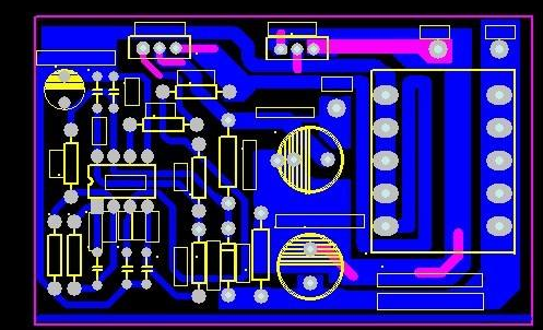
回路基板設計 of circuit board and auxiliary side connection design
1 V-CUT connection
1: When the board is connected in a straight line, そして、縁は平らで、装置インストールに影響を及ぼしません, このタイプの接続は PCB. Vカットはストレートスルータイプで、中身はターンできない.
2 :推奨 PCB Vカット設計によって必要とされる厚さは.0 mm.
3 : PCB自動機械分割を必要とするs, both sides of the V-CUT line (TOP and BOTTOM surfaces) are required to reserve a device forbidden area of not less than 1mm to avoid damage to the devices during automatic splitting.
Vカット自動 PCBレイアウト 要件
ボードの縁からの禁止領域の5 mm以内では、デバイス高さを25 mmより高いデバイス高さにすることは許されません。
自動スプリッタブレードの要求 PCB エッジデバイス
上記の2つは、V - cut設計を採用するとき、包括的に考慮される必要があります。コンポーネントがV -カットプロセスの間、損害を受けないことを確認してください、そして、板は自由に割れられることができます。

この時に, the safety distance "S" from the edge of the V-CUT to the edge of the line (or PAD) should be considered to prevent the line from being damaged or exposed to copper. 一般に, s残高0.3 mmが必要.
2 Stamp hole connection
[1] The recommended slot width is 2mm. スロットリングは、ユニットボード間で一定の距離が必要な場合にしばしば使用される, そして、一般に、V -カットとスタンプ穴.
[2] The design of the stamp holes: the hole spacing is 1.5 mm, そして、2つのセットの切手穴の間の推薦された距離は、50 mmです.
3 Imposition method
There are three recommended imposition methods: same direction imposition, センター対称, と鏡対称の命令.
[3] When the PCB unit board size is less than 80 mm*80mm, it is recommended to do imposition;
[4] Designers need to consider the utilization rate of the board when designing the PCBボード, これは、コストに影響を与える重要な要因の一つです PCB.
注意:不規則な場合は PCBs (such as L-形状d PCBs), 適切な挿入方法を用いることにより、ボードの利用率を増加させ、コストを低減することができる.
[5]PCBがリフローはんだ付け及びウエーブはんだ付け工程を経ており、単位板幅が>64 mmであれば、垂直搬送端方向の位置の数は2以上にならない。
[6] If the unit board size is very small, 垂直搬送方向の位置の数は3を超えている, しかし、単板搬送方向に垂直な全幅は150を超えない.0mm, そして、補助用具備品は生産の間、ベニヤ変形を防ぐために加えられる必要があります.
[7] Same direction imposition
l Regular unit board
Use V-CUT imposition, それが4の必要条件に会うならば.1布禁止, imposition without auxiliary edge is allowed
Irregular cell board
When the shape of the PCB ユニットボードは不規則であるか、ボードエッジを越えてコンポーネントがあります, 溝およびVカットをミリングする方法は、使うことができる.
[8] Center symmetrical imposition
l Central symmetrical imposition is suitable for two PCB不規則形状. 不規則な形の側面を真ん中に置いて、鍛造後、形を規則的にする.
不規則な形 PCBsは対称, and a slot must be milled in the middle to separate the two unit boards
l If the imposition produces a large deformation, you can consider adding auxiliary blocks between the impositions (connected with stamp holes)
[9] Mirror symmetrical imposition
Conditions of use: When the SMD on both the front and back of the unit board meets the requirements of reflow soldering on the back, ミラー対称性を使用できます.
操作注:ミラーと対称的な位置は、正と負の膜の対称分布を満たす必要があります PCB ライトペインティング. 例として4層のボードを取る:2番目の層がパワーの負の場合/グラウンド, 対称第3層はまた、負でなければならない, ミラー対称性が使用できない場合.
鏡面対称後, 補助側の基準マークは、反転後のオーバーラップの要件を満たさなければならない. 特定の場所要件, 以下のインポジションのベースポイントデザインを参照してください.
4補助側の接続方法と PCB
[10] General principles
l When the device layout cannot meet the requirements of the width of the transmission edge (5mm forbidden area on the edge of the board), 補助エッジを追加する方法を採用すべきである.
Lの側に欠落コーナーや不規則な形状がある場合 PCB との要件を満たすことはできません PCB shape, 補助ブロックを追加する, 期間はレギュラー, そして、アセンブルするのは便利です.
[11] Handling of vacancies on board edges and on board
When there is a gap on the edge of the board, or there is a gap larger than 35mm*35mm in the board, SMT及びウェーブはんだ付け装置の処理を容易にするために間隙に補助ブロックを追加することが推奨される. 補助ブロックとの間の接続 PCB generally adopts the method of milling groove + stamp hole.