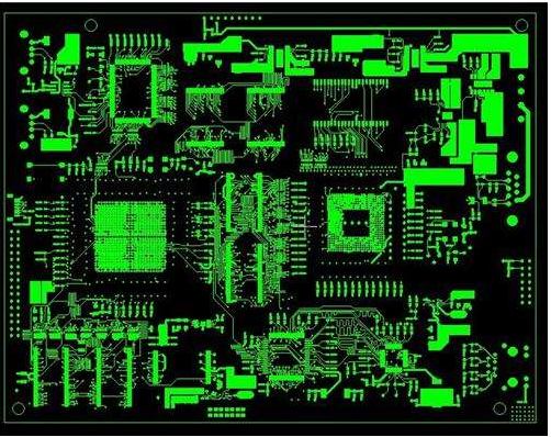
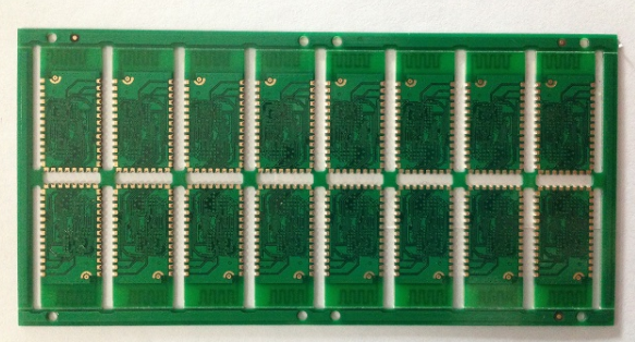
Basic principles and precautions of 回路基板設計
An instrument with good performance, 高品質のコンポーネントと合理的な回路を選択するに加えて, the layout of the components of the 回路基板設計 そして、電気接続方向の正しい構造設計は、器具が確実に動くことができるかどうか決定する重要な問題である. パラメータの同じコンポーネントと回路のために, コンポーネントのレイアウト設計と電気接続の方向が異なる結果を生成する, そして、結果は非常に異なるかもしれません. したがって, の構造を正しく設計する方法の3つの側面を結合する必要があります プリント回路基板 コンポーネントレイアウト, 全体楽器の配線方向とプロセス構造の正しい選択. 合理的なプロセス構造は、不適切な配線に起因するノイズ干渉を除去し、インストールを容易にすることができる, デバッグとメンテナンス.
Below we discuss the PCB回路基板 design 課題. 良い“構造”と“モード”の良い“構造”がないので, 以下の議論は参照のためだけです、そして、参照. The structure of each instrument must be based on specific requirements (electrical performance, overall structure installation and panel layout requirements), 対応する構造設計スキームを採用, といくつかの実行可能な設計スキームを比較して繰り返して.
回路基板電源及びグラウンドバス配線構造選択システム構造:アナログ回路及びデジタル回路は、コンポーネントレイアウトの設計及び配線方法において多くの類似点及び相違点を有する. アナログ回路で, 増幅器の存在のために, the very small noise voltage generated by the wiring will cause serious distortion of the output signal. に digital circuit, TTLノイズ許容値は0です.4V ~ 0.6V, そして、CMOSノイズ耐性は0である.3 of Vcc. ~ 0.45 times, したがって、デジタル回路は強い干渉防止能力を有する.
良い電源とグランドバスモードの合理的な選択は、楽器の信頼性の高い操作のための重要な保証です. かなり多くの干渉源は、電源およびグランドバス12を通じて生成される, そして、接地線に起因する雑音干渉は、最大である.

1. の基本原則要件 回路基板設計
1. Circuit board design starts with determining the size of the board. サイズ プリント回路基板 シャーシシェルのサイズで制限されます. コネクタ, socket or another プリント回路基板). The プリント回路基板 and the external components are generally connected by plastic wires or metal isolation wires. しかし、時々、それはソケットとしても設計されます. プラグインをインストールするには プリント回路基板 装置内, ソケットとして連絡先を残す.
For larger components mounted on the プリント回路基板, 金属アクセサリーは、振動と衝撃耐性を改善するためにそれらを固定するために加えられなければなりません.
2. 基本法 回路基板設計
まず第一に, 仕様を完全に理解する必要がある, 寸法, そして、選択されたコンポーネントおよびさまざまなソケットの領域各構成要素の所在の合理的かつ慎重な配慮, 電磁界両立性と反干渉の観点から. ショートライン, クロスオーバー, power supply, ground path and decoupling are considered. 各々のコンポーネントのポジションが決定されたあと, 各コンポーネントの接続です. 回路図に従って関連ピンを接続する. それを完了する多くの方法があります. 印刷回路図の設計は、2つの方法.
The most primitive is to arrange the layout by hand. これはもっと面倒だ, and it often takes several iterations to complete it. 他の描画装置がない場合も可能である. This manual arrangement of layout methods is also very helpful for those who are just learning the printing plate layout. コンピュータ支援図面, 今、さまざまな機能を持つソフトウェアの描画の多くの種類があります, 一般的に言えば, 図面と変更は、より便利です, そして、彼らは保存されて、印刷されることができます.
Next, 指定したサイズ 回路基板, そして、まず、概略図に従って各構成要素の位置を決定する, その後、連続的な調整後にレイアウトをより合理的にする. コンポーネント間の配線配置 プリント回路基板 is as follows:
(1) Cross circuits are not allowed in the 回路基板設計. 交差する可能性のある線, you can use "drilling" and "winding" to solve them. それで, 他の抵抗器の下でギャップを通って「ドリル」を導く, コンデンサ, 三極ピン, or "wind" from one end of a lead that may cross. In special circumstances, 回路の複雑性, また、設計を簡素化する必要がある. It is allowed to connect with wires to solve the problem of cross circuit.
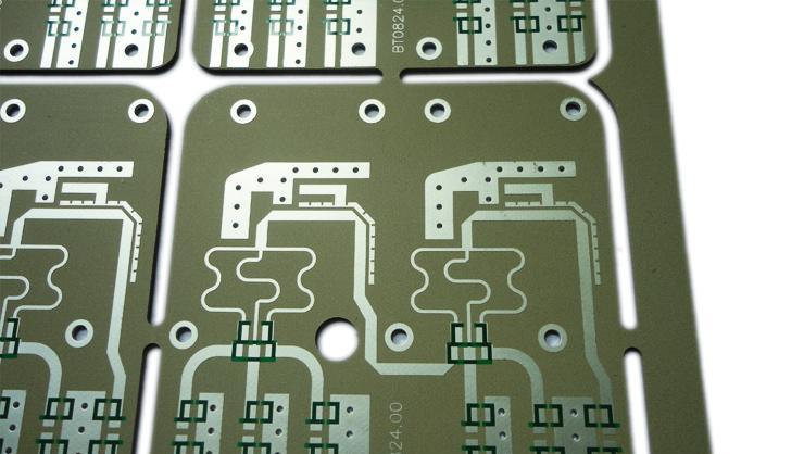
(2) Components such as resistors, diodes, そして、管状コンデンサは、「垂直」と「水平」のインストール方法でインストールされることができます. 垂直型は、部品本体に垂直な構成体の設置及び溶接を指す 回路基板, スペースを節約する利点がある. 水平型は、部品本体の取付及び溶接を、平行にかつその近傍に導く 回路基板, そして、その利点は、コンポーネントのインストールの機械的強度が良いことです. For these two different mounting components, コンポーネントの穴のピッチ プリント回路基板 違う.
(3) In the 回路基板設計, 同じレベル回路の接地点は、できるだけ近いはずである, and the power filter capacitor of this level circuit should also be connected to the grounding point of this level. 特に, the grounding points of the base and emitter of the transistor of this level should not be too far apart, さもなければ、2つの接地点の間の銅箔が長すぎる, which will cause interference and self-excitation. このような“ワンポイント接地方式”回路を使用するとよりよく動作します. Stable and not easily self-excited.
(4) The main 接地線 must be arranged in strict accordance with the principle of high frequency-intermediate frequency-low frequency in the order of weak current to strong current. それをひっくり返してはならない. この要件に従う. In particular, 周波数変換ヘッドの接地線配置要件, regeneration head, 周波数変調ヘッドはもっと厳しい. 不適切であれば, it will self-excite and make it unable to work.
FMヘッドのような高周波回路は、しばしば良好な遮蔽効果を確保するために接地線を囲む大面積を使用する.
(5) Strong current leads (common ground, パワーアンプパワーリード, etc.) should be as wide as possible to reduce wiring resistance and voltage drop, and reduce self-excitation caused by parasitic coupling.
(6) The traces with high impedance should be as short as possible, and the traces with low impedance can be longer, 高いインピーダンスを持つトレースは、信号をホイッスルして吸収しやすく、回路が不安定になるので. The power cord, ground wire, フィードバックコンポーネントのないベーストレース, エミッタリード, etc. すべての低インピーダンストレース. 無線の2つのチャンネルのエミッタフォロワと接地線のベーストレースは分離されなければならない, each in one way, 機能の終了が再び結合されるまで, 二つの接地線が前後に接続されるなら, クロストークを生成し、分離度を低減することは容易である.
2. 以下の点に注意する 回路基板設計
1. の配線方向 回路基板設計: From the perspective of the soldering surface, コンポーネントの配置は、概略図と同様に一貫しているべきである. 配線方向は回路図の配線方向と一致すべきである, 通常、製造工程中に半田付け面に様々なパラメータが必要である. したがって, 検査に便利, debugging and overhaul in production (Note: It refers to the premise that the circuit performance and the installation and panel layout requirements of the whole machine are met).
2. In the 回路基板設計, the arrangement and distribution of various components should be reasonable and even, そして、きちんとしているように努力する, beautiful, 厳格な構造.
3. The 回路基板 重抵抗で設計されている, and the placement of diodes: there are two types: horizontal placement and vertical placement:
(1) Horizontal placement: When the number of circuit components 小さい and the size of the 回路基板 大きいです, 一般的に水平配置を使用する方がよい1以下の抵抗/4 Wは水平に置かれる, the distance between the two pads is general Take 4/10インチ, when the 1/2 Wの抵抗がフラットに配置されます, つのパッドの間の距離は、通常5です/10 inches; when the diode is placed flat, 1 N 400 Xシリーズ整流管, 一般的に3/10 inches; 1N540X series rectifier tubes, 一般的に4〜5/10 inches.
(2) Vertical installation: When there are a large number of circuit components and the size of the 回路基板 is small, 垂直設置は一般に採用される, and the distance between the two pads is generally 1 to 2/垂直インストールの10インチ.
4. Potentiometer: the placement principle of IC holder
(1) Potentiometer: It is used to adjust the output voltage in the voltage regulator, したがって、出力電圧が上昇すると、設計ポテンショメータは時計回りに完全に調整されるべきである, そして、出力電圧が減らされるときに、反時計回りのレギュレータの出力電圧は減少する調整可能な定電流充電器では、中間ポテンショメータは充電電流の大きさを調整するために使用される. ポテンショメータが設計されているとき, ポテンショメータが時計回りに完全に調整されると電流が増加する.
ポテンショメータは、全体の機械構造の設置とパネルのレイアウトの要件を満たす位置に配置する必要があります. したがって, it should be placed on the edge of the board as much as possible, with the rotating handle facing outward.
(2) IC holder: When designing a printed board drawing, ICホルダーを使用する場合, be sure to pay special attention to whether the positioning slot on the IC holder is placed in the correct orientation, そして、各ICピンが正しいかどうか注意を払う, 例えば, 最初のピンは使用できるだけです. それは、ICソケットの右下または左上隅に位置する, and is close to the positioning groove (viewed from the welding surface).
5. Arrangement of in and out terminals
(1) The distance between the two associated lead ends should not be too large, 一般的に2〜3/10インチはより適切です.
(2) The inlet and outlet ends should be concentrated on one or two sides as much as possible, and should not be too discrete.
6. 配線図を設計する際のピン配置順序に注目する, また、コンポーネントピン間隔は合理的でなければならない.
7. Under the premise of ensuring the performance requirements of the circuit, 設計は合理的な配線のために努力すべきである, 外部ジャンパーを使用しない, そして、特定のスムーズな充電条件に従って線を配線してください, そして直感的に努力する, 簡単にインストール, height and overhaul.
8. 配線図の設計, 配線は、曲げられる可能な限り少ない, そして、線は単純で明確でなければなりません.
9. 配線ストリップの幅及び間隔は、適度である, and the spacing between the two pads of the capacitor should be as consistent as possible with the spacing of the capacitor lead pins;
10. The 回路基板 design should be carried out in a certain order, 例えば, 左から右へ、上から下へ.