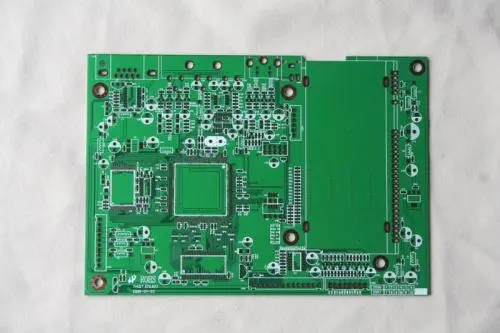
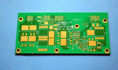
多層PCB回路基板のプロービングプロセス
自動車エレクトロニクスの急速な発展, コミュニケーションエレクトロニクス, 産業管理, 計装, 医用電子, 航空宇宙その他の産業, the 多層PCB回路基板 業界はまた、時々の市場と消費者のニーズを満たしている, そして、時々、工業生産価値の急速な増加を促進します, 多層における競争 PCB回路基板 産業が増加. 多くの回路基板メーカーは、多くの顧客を引き付けるために価格を下げて、消費を誇張するのを躊躇しません. しかし, 低価格PCBボードは低価格材料を使用しなければならない, 生産の質に影響する, 短寿命, そして、製品は外観損傷傾向があります, 衝突と他の品質問題.
多層の目的 PCB回路基板 プルーフは消費者メーカーの強さを決定することである, 多層膜の不良率を効果的に低減できる PCB回路基板s, 将来の大量消費のための確固たる基盤を築く. 多層を見てみましょう PCB回路基板の校正 process.
多層 PCB回路基板 校正工程:
One, contact the circuit board manufacturer
First of all, あなたは、文書のメーカーに通知する必要があります, プロセスリクエスト, 数量. マルチレイヤに必要なパラメータについて PCB回路基板 校正?「注文, そして、消費の進歩を追って.
二番目, open material
Purpose: According to the request of the engineering materials MI, 顧客によって要求されたシートの小さな部分を満たすために、要求を満たす大きなシートを消費者ボードの小さな部分にカットする.
Process: large sheet - cutting board according to MI request - curb board - beer fillet\grinding - board out
Three, drilling
Purpose: According to the engineering materials, 要求されたサイズを満たすシート材の対応する位置に必要な穴直径をドリル加工する.
process: stacked plate pin - upper plate - drilling - lower plate - inspection\repair
Four, Shen copper
Purpose: Copper sinking is the application of chemical methods to deposit a thin layer of copper on the wall of the insulating hole.
process: rough grinding - hanging board - automatic copper immersion line - lower board - dip 1% dilute H2SO4 - thickened copper

Five, graphics transfer
Purpose: Graphic transfer is to transfer the image on the consumer film to the board.
Process: (blue oil process): grinding plate - printing the first side - drying - printing the second side - drying - exploding - shadowing - inspection; (dry film process): hemp board - pressing film - standing - right Position-Exposure-Standing-Development-Check
VI. Graphic plating
Purpose: Pattern electroplating is to electroplate a copper layer with the required thickness and a gold-nickel or tin layer with the required thickness on the exposed copper skin of the circuit pattern or the hole wall.
process: upper board - degreasing - second water washing - micro-etching - water washing - pickling - copper plating - water washing - pickling - tin plating - water washing - lower board
ä¸, Remove the film
Purpose: Use NaOH solution to remove the anti-electroplating masking layer to expose the non-circuit copper layer.
Process: water film: insert rack - soak alkali - rinse - scrub - pass machine; dry film: release board - pass machine
8. Etching
Purpose: Etching is to use chemical reaction to corrode the copper layer of non-circuit parts.
ナイン, green oil
Purpose: Green oil is to transfer the graphic of the green oil film to the board to maintain the circuit and prevent the tin on the circuit when welding parts.
process: grinding plate - printing photosensitive green oil - curium plate - exposure - developing; grinding plate - printing the first side - drying plate - printing the second side - drying plate
å, Character
Purpose: Characters are provided as a mark for easy identification.
Process: After the green oil finishes - cool and stand - adjust the screen - print characters - back
eleven, gold-plated fingers
1. 目的:ニッケルの層をめっきする/プラグの指に必要な厚さの金は、それをより硬く、耐摩耗性にする.
process: upper plate - degreasing - washing twice - micro-etching - washing twice - pickling - copper plating - washing - nickel plating - washing - gold plating
2, tin plate (a process in parallel)
Purpose: Tin spraying is to spray a layer of lead tin on the exposed copper surface that is not covered by solder mask to protect the copper surface from corrosion and oxidation to ensure good soldering performance.
process: micro-erosion - air drying - preheating - rosin coating - solder coating - hot air leveling - air cooling - washing and air drying
12. Forming
Purpose: Organic gongs, ビアボード, ハンドゴング, そして、ダイ・スタンプまたはCNCゴング・マシンによって、手を切ることができます.
明確化:データゴングマシンボードとビールボードの精度が高い, そして、手ゴングは、第2です, そして、最小限の手を切るボードだけのいくつかの簡単な形で行うことができます.
13. Test
Purpose: After electronic 100% testing, 機能に影響する欠陥を検出するには, 視覚的に見つけるのが簡単でない開いた回路と短絡のような.
Process: upper mold - release board - test - pass - FQC visual inspection - unqualified - repair - return test - OK - REJ - scrap
Fourteen, final inspection
Purpose: After 100% visual inspection of board appearance defects, そして、問題と欠陥ボードが流れ出るのを防ぐためにマイナー欠陥を修理するのを止めます.
詳細な作業の流れ:着信材料-表示材料-ビジュアル検査-修飾- fqaスポットチェック-修飾-包装-無資格-処分-点検OK!
デザインの高い技術的な内容のため, 多層の加工と製造 PCB回路基板製造業者. したがって, PCB校正と製造のすべての詳細が正確かつ厳密に行われる限り, 高品質のPCB製品が得られる. より多くの顧客の愛を獲得し、より大きな市場に勝つ.