準備.
回収する PCB設計-related information from the following people

a) Structural design engineer: DXF format files include, (PCB shape, 様々な位置決め穴の位置 PCBボード, 高さ制限面積, 部品が禁止される地域, キーコンポーネントの位置, positions of 様々なボタン and LED And key value).
b) Hardware engineer: schematic diagram, キーライン配線要件, 特殊部品包装要件, etc.
プロジェクト管理:プロジェクト進捗スケジュール.
d) Purchasing department: select PCBメーカー.
生産部門:特殊工程要件の生産. 2. 以下を決定する PCB設計 パラメータ.
板厚.
Circuit board stack structure (distribution of power layer, ground layer and signal layer).
バイアの種類.
d) Circuit board material and dielectric constant.
デフォルトの線幅と線間隔.
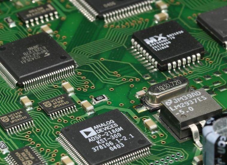
2. Check the device package
1. 回路図をPCBにインポートします.
エラーレポートの情報をチェックする.
3. Check the package for errors (especially the devices newly added to the package library).
分極デバイスの極性をチェック.
5. バックアップ回路図.
回路の間違ったデバイスを置き換える. 対応する装置がなければ, 新しいデバイスライブラリを作成するために.
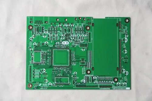
3. 回路基板の基本情報を作成する.
. DXFファイルを非配線層にインポートする. (Check the drawing scale and key dimensions)
2. Draw the outer frame of the circuit board according to the DXF file (線幅 0.1 mm).
3. 回路基板の外形寸法に応じてボードとボードの大きさに加わる方法を決定する.
4. Create an outline layer and draw the outer frame of the puzzle (line width 0.1mm) on this layer.
5. Add positioning holes (4mm diameter non-metalized holes).
6. マークポイントを追加.
7. パネルのポイントを追加.
8. Add label text on the PANEL frame (PART NUMBER and TOP, BOTTOM label)
Fourth, デバイスレイアウト.
1. ハードウェアエンジニアとの全体的なレイアウト計画.
2. 構造エンジニアによって必要とされる位置決め穴を加えてください.
3. 主なコンポーネントを配置する, various buttons, LEDs, etc. 組織の要件に従って.
4. 機能ブロックによるレイアウトとネットワーク関係.
5. 構造要件を使用して任意の矛盾のレイアウトとデバイスの高さをチェックします.
6. デバイスのギャップがルールと一致するかどうか、デバイスのオーバーラップがあるかどうかを確認します.
7. ボードのポイントを追加.
8. 検査のための1 : 1組立図面を印刷する.
9. DXFファイルを生成し、構造的な問題があるかどうかを確認するために構造エンジニアに提出します.
構造の競合を変更.
ファイブ, add silk screen
1. シルクスクリーンの幅は最小0です.15 mm.
2. シルクスクリーンテキストの最小高さは1です.mm.
3. 底面テキストがミラーされて.
4. すべての絹の画面の内容は、パッドと露出銅箔をカバーしていません.
六, wiring
1. 配線規則.
デフォルトのギャップ, line width.
b) Special network gap and line width.
c) The power and ground wires fill the gaps.
2. マニュアル配線.
a) Follow the wiring rules for wiring.
b) The key line decides the wiring method together with the hardware engineer.
c) Work with the hardware engineer to determine the power cord routing method.
3. 電力と接地線充填を加える.
a) Determine the filling area together with the hardware engineer.
b) Keep a gap of at least 0.充填領域と基板の縁部との間の25 mm.
充填エリア内の同じネットワーク内のすべてのビアがオーバーレイ充填に設定されます, フラワーホール接続は使用しません.
充填エリアのすべての同じネットワークパッドは、十字形の熱パッドによって接続されます.
4. 地面バイアを加える.
a) Add grounding vias in the gaps of the circuit, そして、すべての層の接地線を均一に充填しようとする.
b) Add grounding vias along both sides of the audio line to ensure the shielding effect
c) Add grounding vias along the edge of the PCBボード ESD効果を確実にする.
5. run ruleすべてのエラーレポートをチェックする.
6. 接続チェックを実行し、ネットワーク接続を接続しません.
7. レビューを行うために関連する人事を整理する.
8. スタンプ穴を追加し、フライスカッターパスを描画.
1. 切手穴を加える.
すべての穴とワイヤの間のクリアランスは、0以下であること.25 mm.
b) The clearance between all drill holes and pads shall not be less than 0.30 mm.
c) Set stamp holes as evenly as possible on both sides of the PCB.
d) The stamp hole shall not be set near the devices with protruding board edges (such as side buttons, イヤホンソケット, etc.).
2. フライスカッターのパスを描画する.
フライスカッターのミーリングパスを0の線幅でボードエッジの中心線に沿って描画します.1mm.
b) The start and end of the path are the centers of the exit holes on both sides of the stamp hole.
9. 出力装置, y座標ファイル.
1. パワーPCBユニットをメートル法に設定する.
2. デバイスXの作成, y座標ファイルでそれらを保存します.
10. 出力カムファイル.
1. 出力形式を設定する.
a) GEBER file: RS-274-X, 3時5分, 単位=英語.
b) NC Drill file: Out Type=ASCII, 3時5分, 単位=英語.
2. 各層の出力内容を設定する.
a) Signal layer: Pads, 跡, ヴィアス, 銅, 銅とピン.
b) Solder mask: Pads, 銅, ライン, テキスト, 銅とピン.
c) Solder paste layer: Pads, 銅, ライン, 銅とピン.
d) Silk screen layer: Copper, ライン, テキスト.
e) OutLine: Lines.
f) Mill: Lines.
穴のレイヤーに応じて設定を定義します. メタライズスルーホールと非メタライズスルーホールは別々に出力される.
3. 出力ファイルの種類が完了したかどうかを調べる.
4. エクスポートカムファイル.
11. Cam 350でガーバーファイルをインポートします.
1. すべてのGerberデータをインポートするAutoimport.
2. インポートされたグラフィックスをチェックする.
3. に従って掘削サイズを設定します .ガーバーファイルのREPファイル.
4. すべてのDコードを0のサイズで削除します.
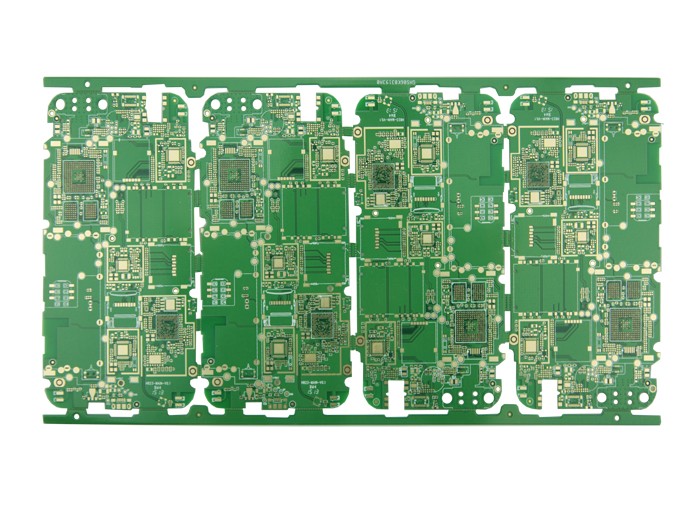
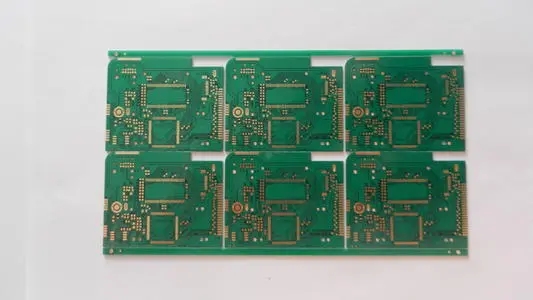
12. ジグソーパズル.
1. PCBをコピーして.
2. ミラーの後のグラフィックスの各層をチェックする. 3. ミルツールをミルツールにミル層グラフィックスをミルパスに変換する. フライス盤の幅は63 milである.
4. 計算された座標位置に従ってPCBをパネルにコピーする.
5. パズル全体をチェック.
13. 輸出ガーバーファイルとNCドリルファイル.
14. 検査のためのガーバーファイルとNCドリルファイルをインポートする.
15. 処理ファイルをzip形式に圧縮する.