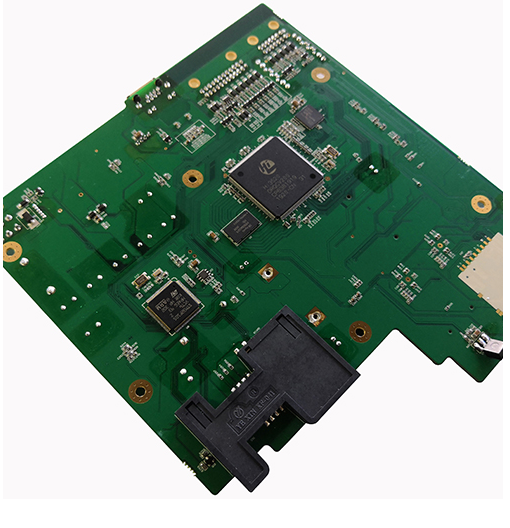
の指示は何ですか PCBA 加工外観検査
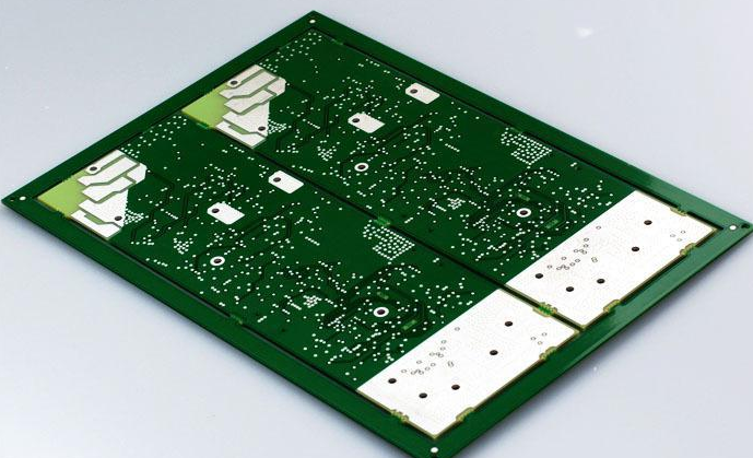
PCBA プリント回路基板の処理, プリント回路基板, プリント回路基板, 英語の略語を使う PCBA, 重要な電子部品, 電子部品の支援, 電子部品用回路接続装置. 電子印刷技術を使用して作られているので, プリント回路板と呼ばれる. プリント回路基板の出現以前, 電子部品間の相互接続は、完全な回路を形成するためにワイヤの直接接続に依存した.
現在, 回路ブレッドボードは効果的な実験ツールとして存在する, そして、プリント回路基板は、エレクトロニクス産業の絶対支配的な位置になりました. しかし、ほとんどの人はまだ PCBA 加工外観検査指示? の編集者とそれについて学びましょう PCBA処理.
PCBA処理外観検査命令

⢠Missing parts: The components are not mounted as required in the corresponding position on the PCBA.
空のはんだ付け:空のはんだ付け:3/4 of the area of the solder joints with no or less solder on the component feet (SMD components are less than 1/2 of the width of the component).
Lian tin :異常操作のため, 元々接続されていなかった2点は、錫とつながっていた.
誤った部分は間違っています:部品は PCBA do not match those shown on the BOM
⢠Welding: The component pins are not well tinned, and effective welding cannot be guaranteed (including false welding)
⢠Cold welding: The surface of the solder joint is gray without good wetting.
コンポーネントがマウントされた後, the polarity is opposite to that specified in the document
⢠Tombstone: One end of the patch component is lifted away from the pad to form a tombstone
⢠Back: The front of the module (the silk-screened side) is facing down, but the welding is normal
⢠Open circuit: the component pin is disconnected or the circuit on the PCBA board is disconnected
⢠Tombstone: One end of the patch component is lifted away from the pad to form a tombstone
⢠Back: The front of the module (the silk-screened side) is facing down, but the welding is normal
⢠Open circuit: the component pin is disconnected or the circuit on the PCBA board is disconnected
⢠Lifting: The copper foil or pad of the circuit is lifted from the PCBA surface and exceeds the specification
⢠Multiple pieces: The file indicates the location of no components, に対応するコンポーネントがあります PCBA board
⢠Tin cracking: usually after the solder joint is subjected to external force, はんだ接合部および部品ピンは分離される, はんだ付け効果や隠れた危険に影響を及ぼす. 当社の工場は中国に位置しています. 何十年も, Shenzhen has been known as the world's electronics R&D and manufacturing center. 当社の工場やウェブサイトは、中国政府によって承認されて, それで、あなたはMiddlemenをスキップして、自信で我々のウェブサイトで製品を買います. 我々は直接工場だから, これが私たちの古い顧客の100 %が100 %を購入し続ける理由ですIPCB. あなたは私たちから1. 私たちはあなたが本当にお金を節約する必要はありませんものを購入することを強制されません.
Free DFM
Before you pay in the most timely manner, すべてのご注文は、我々のよく訓練された専門家と技術者による無料のエンジニアリング文書レビューサービスを受けます.