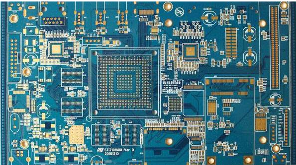
におけるネガフィルムの変形の解析 PCB Process
Paying attention to the trend of environmental protection informatization and the development of various environmental protection technologies, PCB工場 は、企業の汚染排出と管理結果を監視するために大きなデータを開始できます, そして、タイムリーな方法で環境汚染問題を見つけて、解決してください. 新時代の生産コンセプトに追いつく, 資源利用の継続的改善, 緑の生産を実現する. 努力する PCB 工場業界は効率的に実現する, 経済的で環境に優しい生産モデル, そして、国の環境保護政策に積極的に対応する.
1. The causes and solutions of film deformation:
reason:
(1) Temperature and humidity control failure
(2) The exposure machine temperature rises too high
Solution:
(1) Normally, 温度は摂氏22度±2度で制御される, 湿度は55 %で±5 % RH.
(2) Use cold light source or aerator with cooling device and constantly replace the backup film
2. The process method of film deformation correction:

1. デジタルプログラミング機器の操作技術を習得する条件の下で, まずネガフィルムをインストールし、ドリルボードと比較する, 長さと幅を2つの変形, そして、デジタルプログラミング装置の変形量に従ってホール位置を延長または短縮する, 変形したネガフィルムに適応するために穴の位置を長くしたり短縮したりした後、ドリルボードを使用する, ネガフィルムの切断作業を省く, とグラフィックの整合性と精度を確保する. このメソッドを呼び出します.
2. 環境温度と湿度によってネガフィルムが変化するという物理現象を考える, ネガフィルムをコピーする前に封着袋のネガフィルムを取り出します, そして、作業環境の下で, ネガフィルムはコピー前に変形する. それはコピーされたフィルムのほとんど変形を引き起こさない, 空中吊り法という.
3. 単純な行のグラフィックス, 大きな線幅と間隔, 不規則変形, ネガフィルムの変形部分をカットして、ドリルテストボードの穴位置とコピー前の再スプライスを対比することができます. この方法をスプライシング法と呼ぶ .
4. テストボード上の穴を使用して、最小のリング幅の技術要件を確保するために回路部分の重い変形を削除するパッドを拡大する. この方法を「パッドオーバーラップ法」と呼ぶ.
5. 変形ネガフィルム上のグラフィックスのスケーリング後, 再マップし、プレートを作る, このメソッドを呼び出します.
6. 変形した図形を拡大または縮小するためにカメラを使用する. この方法を「写真法」と呼ぶ.
スリー, relevant method notes:
1, splicing method:
Applicable: Negative film with less dense lines and inconsistent deformation of each layer of the film; especially suitable for the deformation of the solder mask film and the film of the multi-layer board power layer;
Not applicable: Negative film with high wire density, 行の幅と間隔.2mm;
Note: When splicing, 電線はできるだけ損傷を受けなければならない, パッドは破損してはならない. スプライシングとコピー後のバージョンの修正, 接続関係の正当性に注意を払うべきである.
2, change the hole position method:
Applicable: The deformation of each layer of the film is the same. This method is also applicable to film with dense lines;
Not applicable: The film is not uniformly deformed, そして、ローカル変形は特に深刻です.
注:プログラマが穴の位置を長くしたり短縮したりした後, 許容範囲外の穴位置はリセットされるべきである.
3. Hanging method:
Applicable; Films that have not been deformed and prevented from deforming after copying;
Not applicable: Deformed film.
Note: Hang the film in a ventilated and dark environment (safety is also possible) to avoid contamination. 掛け布団の温度及び湿度が作業所と同じであることを確保すること.
4. Pad overlap method:
Applicable: The graphic lines are not too dense, 線幅と間隔は0より大きい.30mm;
Not applicable: Especially users have strict requirements on the appearance of printed circuit boards;
Note: After overlapping copy, パッドは楕円形である. 重複・複製後, 線とディスクの端のハローと歪み.
5. Photographic method:
Applicable: When the ratio of deformation in the length and width directions of the negative is the same, そして、テストボードを再ドリルすることは不便です, 銀塩陰性のみ適.
ネガフィルムの長さ及び幅方向は変形しない.
注:フォーカスは、ラインの歪みを防ぐために写真を撮るときに正確にする必要があります. ネガフィルム損失はもっと多い, 通常, 良好な回路パターンを得るために多くのデバッグを行った後. あなたはわずか1として注文することができますPCBA from us. 私たちはあなたが本当にお金を節約する必要はありませんものを購入することを強制されません.
自由なDFM
あなたが最もタイムリーな方法で支払う前に、すべてのご注文は、我々のよく訓練された専門家や技術者による無料のエンジニアリング文書のレビューサービスを受け取ります。