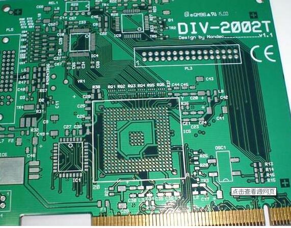
(1) The package of the components used on the PCB 正しくなければなりません, コンポーネントピンのサイズとサイズを含む, ピンの間隔, ピンの数, 枠の大きさと方向, etc.
(2) The positive and negative poles or pin numbers of polar components (electrolytic capacitors, ダイオード, 三極, etc.) should be marked in the PCB コンポーネントライブラリと PCBボード.
(3) The pin numbers of the components in the PCBライブラリ should be consistent with the pin numbers of the schematic components.
(4) For components that require heat sinks, コンポーネントパッケージを描画するときにヒートシンクのサイズを考慮しなければならない, そして、コンポーネントおよびヒートシンクは、全体的なパッケージ形式に一緒に引き寄せられることが可能である.

(5)部品とパッドとのピンの内径を一致させ、パッドの内径を部品のピンサイズよりも若干大きくし、設置を容易にする。
2. 要件 PCB component layout
(1) The components are arranged uniformly, そして、同じ機能モジュールの構成要素は、できるだけ近くに配置されるべきである.
(2) The components using the same type of power supply and ground network should be arranged together as much as possible, これらは、内部電気層を介して互いの間の電気的接続を完了するのに有益である.
(3) The interface components should be placed aside, また、文字列でインタフェースタイプを示さなければなりません, そして、配線の方向は、通常回路基板から離れていなければならない.
(4) Power conversion components (such as transformers, 直流/直流変換器, 3端子レギュレータ管, etc.) should have enough space for heat dissipation.
(5) The pins or reference points of the components should be placed on the grid point, 配線と美学に資するもの.
(6) The filter capacitor can be placed on the back of the chip, チップの電源とグランドピンの近くに.
(7) The first pin of the component or the sign indicating the direction should be marked on the PCBボード and cannot be covered by the component.
(8) The label of the component should be close to the component frame, サイズが揃っている, 方向にきちんと, パッドとビアと重複しない, コンポーネントがインストールされた後にカバーされた領域に配置できません.