(1) Power supplies of different voltage levels should be isolated, 電源線は交差すべきではない.
(2) The wiring adopts 45° corners or circular arc corners, 鋭いコーナーは許されない.
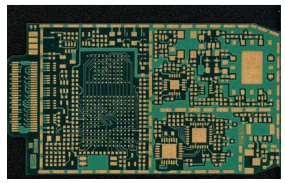
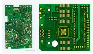
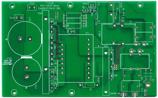
8b460e042b313f49cfeeffb1c.png "pcb board")
(3) The PCB トレースは直接パッドの中心に接続されます, そして、パッドに接続しているワイヤの幅は、パッドの外径を超えることができない.
(4) The line width of the high-frequency signal line is not less than 20mil, そして、それを囲むために外部接地線が使用される, 他の接地線から隔離される.
(5) Do not wire the bottom of the interference source (DC/直流変換器, 水晶発振器, 変圧器, etc.) to avoid interference.
(6) Thicken the power line and ground line as much as possible, そして、スペースが許すならば、電力線の幅は50ミル.
(7) The signal line width of low voltage and low current is 9ï½30mil, そして、スペースが許すならば、それはできるだけ厚くなければなりません.
(8) The spacing between signal lines should be greater than 10 mils, そして、電力線の間の間隔は、20マイル.
(9) The line width of high-current signal lines should be greater than 40 mils, そして、間隔は30マイル.
(10) The minimum size of the via hole is preferably 40 mil outside diameter and 28 mil inside diameter. 上部層と底層との間の配線と接続する場合, パッドが好ましい.
(11) It is not allowed to arrange signal lines on the inner 電気層.
(12) The width of the interval between different areas of the inner electrical layer shall not be less than 40 mils.
(13) When drawing the boundary, 境界線を接続する領域のパッドを通過させないようにしてください.
(14) Laying copper on the top and bottom layers, それは完全に空のスペースをカバーし、死んだ銅を残してグリッド幅よりも線幅の値を設定することをお勧めします. 同時に, keep a distance of more than 30mil (0.762mm) from other lines (copper can be used in the Set the safety distance before, and change it back to the original safety distance after the copper coating is completed).
(15) Teardrop the pad after wiring.
(16) The metal shell device and the external grounding of the module.
(17) Place the pads for mounting and soldering.
(18) The DRC check is correct.
4. PCB層 requirements
(1) The power plane should be close to the ground plane, 地面にしっかりと結合している, グランドプレーンの下に配置.
(2) The signal layer should be adjacent to the inner electrical layer, 他の信号層に直接隣接しない.
(3) デジタル回路分離 アナログ回路. 条件なら, アナログ信号線とデジタル信号線を層に配置し、遮蔽対策を採用する彼らが同じ信号層に配置される必要があるなら, 干渉を減らすために分離帯域と接地線を使用する必要があるアナログ回路及びデジタル回路及びグランド用の電源は互いに分離され、混合することができない.
(4) The high-frequency circuit has a large external interference, そして、それを別々に配置するのがベストです, そして、内側に直接隣接する中間信号層を使用する 電気層 伝送のために上下の, 内側の銅膜を使用するために 電気層 外部干渉を減らす.