PCB生産プロセスフローチャートの多くの種類があります. 回路基板のレイヤーのナンバーおよび回路基板の生産プロセスによれば, に分けます。 両面回路基板 プロセスフロー, 多層回路基板プロセスフロー, PCB銅めっきプロセス, 数値制御旋盤加工プロセス, PCBはラインパターン転送と形状処理のためのいくつかの主要な生産プロセスがある.
The basic manufacturing process of the factory to produce PCB circuit boards
Printed boards can be divided into single-sided, 導体パターンの層数に応じた両面プリント板. The basic manufacturing process of a single panel is as follows:
Foil-clad board-->Unloading-->Baking board (to prevent deformation)-->Mould making-->Washing, drying-->Film (or screen printing) ->Exposure and development (or anti-corrosion ink)- ->Etching-->Film removal--->Electrical continuity inspection-->Cleaning treatment-->Screen printing solder mask pattern (printed with green oil)-->Curing-->Screen printing marking symbols-->Curing- ->Drilling-->Shape Processing-->Cleaning and Drying-->Inspection-->Packaging-->Finished Product.
The basic manufacturing process of double-sided panels is as follows:
In recent years, 両面プリント配線板の製造方法としては、SMORC法とパターンめっき法がある. 特定の機会に, プロセスワイヤ方式も使用される.

1. Graphic electroplating process
Foil Clad Laminate-->Cutting-->Punching and Drilling Benchmark Holes-->CNC Drilling-->Inspection-->Deburring-->Electroless Plating Thin Copper-->Plating Thin Copper-->Inspecting--> Brushing-->Filming (or screen printing)-->Exposure and developing (or curing)-->Inspection and repairing-->Pattern plating (Cn ten Sn/Pb)-->Removing film-->Etching- ->Inspect and repair the board-->Plug nickel-plated gold- ->Curing-->Shape Processing-->Cleaning and Drying-->Inspection-->Packaging-->Finished Product.
過程で, the two processes of "electroless plating of thin copper --> electroplating of thin copper" can be replaced by a single process of "electroless plating of thick copper", 両方の利点と欠点がある. パターン電気めっき---両面に金属化した板を製造するためのエッチング方法は1960年代と1970年代の典型的プロセスである. 1980年代半ば, the bare copper-clad solder mask process (SMOBC) gradually developed, 特に精密両面パネル製造において主流プロセスとなっている.
2. Bare Copper Clad Solder Mask (SMOBC) process
The main advantage of SMOBC board is that it solves the short-circuit phenomenon of solder bridging between thin lines. 同時に, 鉛と錫の一定比により, これは、ホットメルトボードよりも優れたはんだ付け性とストレージ特性を持って.
SMOMCボードを製造する多くの方法がある, 標準パターン電気メッキ減算とリードすずストリッピングのSmobcプロセスを含む鉛めっきの電気めっきの代わりにスズめっきまたは浸漬スズを使用する減法パターン電気めっきSMOCプロセスプラグまたはマスキングホールSMOCプロセス;添加法SMORC技術等. 以下、主に、SMORCプロセスおよびパターン電気メッキ法のプラグド法Smobcプロセスフローおよびそれからリード及びスズストリッピングを導入する.
パターン電気めっきのSMORCプロセスはリードおよびスズストリッピング後のパターン電気めっきプロセスと類似している. エッチング後のみ変化.
Double-sided copper clad board-->According to the pattern electroplating process to the etching process-->Pb-Sn-->Inspection-->Cleaning--->Solder mask pattern-->Plug nickel plating and gold plating--> Adhesive tape for plugs-->Hot air leveling-->Cleaning--->Screen printing mark symbols--->Shape processing--->Cleaning and drying--->finished product inspection-->Packaging-->finished product.
PCB process
The film bottom plate is the leading process of プリント回路基板 production, そして、フィルム底板の品質は、直接の生産品質に影響を及ぼします プリント回路基板. ある種の プリント回路基板, 少なくとも1つのセットの対応するフィルムマスターズがなければなりません. Each kind of conductive pattern (signal layer circuit pattern and ground, power layer pattern) and non-conductive pattern (solder mask pattern and character) of the printed board should have at least one film negative. 光化学転写過程, 様々なパターンが生産ボードに移される.
フィルムマスターズの使用 プリント回路基板 production are as follows:
The photosensitive mask patterns in pattern transfer include circuit patterns and photoresist patterns.
スクリーン印刷プロセスにおけるスクリーンテンプレートの作成, はんだマスクグラフィックスと文字を含む.
Machining (ドリル and profile milling) CNC machine tool programming basis and drilling reference.
エレクトロニクス産業の発展に伴い, プリント板の要求はますます高くなっている. 高密度, 細線, プリント基板の小開口設計は、より速く、より速くなる傾向がある, そして、プリント基板の製造工程はますます完璧になってきている. この場合は, 高品質の映画マスターがなければ, 高品質 プリント回路基板sは生産できる. The production of modern printed boards requires the film master to meet the following conditions:
The dimensional accuracy of the film master must be consistent with the accuracy required by the printed board, そして、製造工程に起因する偏差を考慮して補償を行うべきである.
フィルムベースのグラフィックスは設計要件を満たすべきである, グラフィックシンボルは完了する必要があります.
フィルムマスターのグラフィックのエッジはストレートできちんとしている, エッジは想像上ではありません。黒と白のコントラストは大きい, 感光性プロセスの要件を満たす.
フィルム基材は、寸法安定性が良好でなければならない, それで, 周囲温度と湿度の変化による小寸法変化.
両面および多層ボードのフィルムマスターズはパッドと共通パターンの良好な重なりを必要とする.
フィルムマスターの各層は明確にマークされるか、または命名されるべきです.
フィルムベースは、必要な光の波長を送信することができる, 一般的な感光性に必要な波長範囲は、3000〜4000 Aである.
過去に, 映画マスターズを作るとき, これは、一般的にフォトマスターを最初に生成する必要があった, その後、写真や海賊を使用してフィルムマスターの生産を完了する. 今年, コンピュータ技術の急速な発展, フィルムマスターズの制作工程も大幅に発展している. 高度なレーザー光塗装技術の使用は大幅に生産速度とマスターの品質を向上させる, 高精度を作り出すことができる, 過去に完成できなかった針金模様, making the CAM technology of printed board production tend to be perfect
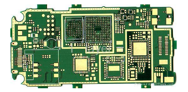
Copper Clad Laminates (Copper Clad Laminates, abbreviated as CCL), 銅張積層板又は銅張積層板, 製造用基板材料 プリント回路基板s (hereinafter referred to as PCB). 現在, エッチング方法によって製造された最も広く使用されるPCBは、必要な回路のパターンを得るために銅クラッド基板上に選択的にエッチングすることである. 銅張積層体は主に伝導の3つの機能に対して責任がある, 絶縁とサポート全体 プリント回路基板. 演奏, プリント板の品質と製造コストは銅張積層板に大きく依存する.
The main process flow of the plugging method is as follows:
Double-sided Foil Clad Laminate-->Drilling-->Chemical Copper Plating-->Plating Copper on the Whole Board-->Blocking Holes-->Screen Printing Imaging (Erect Image)-->Etching-->Removing Screen Printing, Remove plugging material-->Cleaning-->Solder mask pattern-->Plug nickel plating, gold plating-->Plug tape tape-->Hot air leveling-->The following procedures are the same as the above to the finished product.
このプロセスの工程は比較的単純である, そして、キーは穴を塞いで、穴をふさぐインクをきれいにすることです.
穴詰まり過程で, 穴をふさぐインクとスクリーン印刷イメージングが使われないならば, 特別なマスキングドライフィルムは、ホールをカバーするために使用されます, そして、肯定的なイメージを作るために露出する, これがマスキングホールプロセス. ホールブロッキング法と比較して, それはもはや穴にインクを洗浄する問題がある, しかし、それはドライフィルムをマスキングするためのより高い要件を持っています.
SMORCプロセスの基礎は、最初に裸の銅穴メタライズされた両面基板を製造することである, その後、熱風平準化プロセスを適用する.
PCB engineering production
For the production of プリント基板, 多くのデザイナーが回路基板の製造プロセスを理解していないので, それらによって設計された回路図は最も基本的な回路図だけであり、生産に直接使用することはできない. したがって, 実際の生産の前に回路ファイルを修正・編集する必要がある. だけでなく、工場の生産プロセスに適した映画チャートを作成する必要があります, また、対応するパンチデータを生成する必要があります, 金型データ, その他の生産に役立つデータ. それは直接様々な将来の生産プロジェクトに関連している. これらのすべては、必要な生産プロセスとマスター関連のソフトウェア生産を理解するためにエンジニアリングと技術者を必要とします, などの一般的な回路設計ソフトウェアを含む, PADS 2000, オートキャド, etc., また、などの必要なCAMソフトウェアに精通している:View 2001, カム350 ;GCCAMなど, CAMは、PCB設計入力を含むべきです, エディット, 正しい, 回路グラフィックスの修理と付与, 媒体としてディスクを使う, そして、描画のための自動データを出力する, drilling, とテスト.