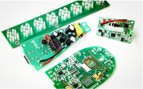
検査目的:製造された製品のはんだ接合強度の信頼性を検証する PCBA.
検査方法及び工程
はんだ接合部の目視検査
(1) Use tools: X-Ray, 3-D microscope
(2) Main inspection, ハンダボールはんだ接合形状を主に検査するX線, 短絡回路, 変位, 空隙サイズ, etc. BGAの, LGA, QFNと他の部分;三次元顕微鏡は主に鉛漏れ部品のはんだ接合の外観を検査する, 半田付け角度. etc., BGA部品周辺における錫球の外観, すず亀裂, 盗品, etc.
(3) Inspection frequency: X-Ray: For BGA and LGA products, 1 pannelは1 k毎に検査される. 3次元顕微鏡を導入した: BGAとLGA第1ピース, 四面と中心の5つの粒子の外観が検査される. Used when analyzing defective products
(4) Inspection standard: Acceptance standard of Void size
IPC610D specification:
1. The bubble volume ⤠25 % of the tin ball volume is the acceptable bubble acceptance standard:
2. The bubble volume ⥠25% of the tin ball volume is unacceptable
Solder Balls displacement judgment standard:
1: Solder ball offset PADâ¤25% is an acceptable level
2: Solder ball offset PADâ¥25% is unacceptable
Solder Balls Short Circuit Judgment Criteria: All short circuits are unacceptable even with tin
2. Solder joint strength inspection
(1) Tools used: push-pull machine and fixture
(2) Main inspection: resistance/静電容量/inductance/芝, QFPと他のオリジナルプッシュプル力測定. 検査周波数:新製品検査/新しいオリジナル/new solder paste is introduced; when bad analysis
(3) Inspection standards: There are currently no inspection standards and empirical values in the industry, 顧客だけの要件を除いて.

3. Dye test
(1) Tools used: dye, 真空ポンプ, オーブン, 3-D microscope
(2) Main inspection: Whether the tin balls of BGA parts are intact and whether there is tin cracking
(3) Inspection frequency: inspection at the time of new product/新しいオリジナル/新しいはんだペースト導入; at the time of failure analysis
(4) Inspection standards:
Crack (color display) is not allowed on PCBA それは信頼性実験を行わなかった.
PCBA はんだ接合端層に信頼性実験を行った後、クラック.
4. Section Inspection
(1) Use tools: grinding machine, シール材, サンドペーパー, polishing powder
(2) Main inspection: Cross-section observe the metallographic structure of the solder joints, はんだ接合部のIMC成形と結晶化.
(3) Inspection frequency: inspection at the time of new product/新しいオリジナル/new solder paste introduction; at the time of failure analysis
(4) Inspection standards:
Slice Solder Ball, QFP, SOP sample inspection:
1: Solder ball offset PADâ¤25% is an acceptable level
2: Solder ball offset PADâ¥25% is unacceptable
3: Both short-circuit and empty welding at the solder joint ends are rejected.
4: Crack not allowed
5. Microstructure and element analysis
(1) Use tools: SEM electron microscope & EDX
(2) Main inspection: microstructure of solder joints, 厚さ測定, and surface element structure analysis
(3) Inspection frequency: inspection at the time of new product/新しいオリジナル/new solder paste introduction, and at the time of failure analysis
(4) Inspection standard: Solder Joint IMC thickness inspection:
PCBA パッド端:2 - 5 um, Component Substrate 1-3um
EDX judgment: usually Solder Ball and element composition are: Sn/エージー/Cu 96.5%/3.0/0.cとoの原子比が10 %で正常である5. IMC層のエレメントPの含有量は、約9〜11 %である, どちらが正常か.