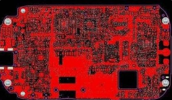
p>Analysis of high frequency circuit in CAD
When the operating frequency is higher (about 2GHz), 信号波長はデバイスサイズと徐々に一致する. チップインダクタのインピーダンスは明らかな分布特性を示す, それで, 異なる参照位置に異なるインピーダンスが存在する. 高周波で, デバイスの回路応答はその大きさと空間構造によって変化する. 従来のインピーダンス測定パラメータは実際の回路の応答特性を正確に反映できない. 携帯電話のRF電力増幅回路の一例としての検討, two high-frequency inductors (working frequency 1.9GHz) used for impedance matching are photolithographic thin-film inductors. If the laminated chip inductors (measuring instrument hp-4291b) with the same specifications and accuracy but significantly higher Q value are replaced, 回路の伝送利得はほぼ10 %低下する. これは、回路の整合状態が低下していることを示す. 低周波数解析法を用いて高周波の応用を正確に説明できないことは明らかである. それは適切ではない, 少なくとも十分ではない, LおよびQを有するチップインダクタの高周波数解析に注目する.
電磁場理論はしばしば工学における分布特性を持つ高周波数応用問題を解析するために使用される. 一般に, in the measurement of chip inductor by impedance analyzer (hp-4291b), 測定精度は約0.固定具補償と計器キャリブレーションによる1 NH, 回路設計の精度要件を理論的に保証するのに十分である. しかし, the problem that can not be ignored is that the measurement results at this time only reflect the parameter performance between the end electrode interfaces of the inductance device under the matching state (the measuring fixture is designed to accurately match), しかし、インダクタンス装置の内部電磁分布及び外部電磁環境要件は反映されない. 同じテストパラメータを有するインダクタは、異なる内部電極構造に起因する完全に異なる電磁分布を有することができる. 高周波条件下で, the actual circuit application environment (approximate matching, 密集, PCB distribution influence) of chip inductors is often different from the test environment. 様々な複雑な近接場反射を生成するのは非常に簡単である, resulting in slight changes of actual response parameters (L, q). RF回路における低インダクタンスのために, この影響は無視できない, 我々はそれを「分散影響」と呼びます.
In the design of high-frequency circuit (including high-speed digital circuit), 回路性能を考える, デバイス選択と電磁両立性, the working performance of the actual circuit system is generally considered by means of network scattering analysis (s parameter), 信号完全性解析, 電磁界解析, 回路シミュレーション解析, etc. チップインダクタの「分散影響」問題の観点から, 実現可能な解決策は、インダクタの構造電磁シミュレーションを行い、回路設計の基礎として対応するSPICE回路モデルパラメータを正確に抽出することである, 高周波設計応用におけるインダクタンス素子の誤差影響を効果的に低減するために. Most of the technical parameters of chip inductors produced by foreign (Japanese) main component enterprises contain s parameter, これは正確な高周波数解析解析に使用できる.