The line drawn by TopLayer (top layer) is red, 大将の上層 両面板, そして、このレイヤーは、片面の板のために使われません.
The line drawn by BottomLayer (bottom layer) is blue, これは、単一のパネルの上のライン層です.
MidLayer1 (MidLayer1) This is the first middle layer. 30層があるらしい. 一般に, デザイナーは使えない. 心配する必要はない. 複数のパネルがある場合に使用されます. デフォルトは99 seでは表示されません, 使用しない.
Mechanical Layers (purple red) are used to mark the size と board description, は PCBコピー板 処理, それで, ボードは見えないときは見えない, 簡単な点注釈.
Top Overlay (the top silk screen layer) (yellow) is the characters on the front of the board. This layer of characters can be used for the TopLayer (top layer) single panel. The Bottom Overlay (bottom screen layer) (brown) corresponds to the BottomLayer (bottom layer), どちらが板ですか. 背中の文字のために, 上記2層の文字は両面で使用される.
KeepOutLayer (prohibited wiring layer) (purple red with the mechanical layer) is simply the frame and appearance of the board.
Multi layer (multi-layer) (silver) All wiring layers are included. 一般に, シングルおよび両面プラグインパッドはこの層にあります, ストライプはすべての層に描かれている.
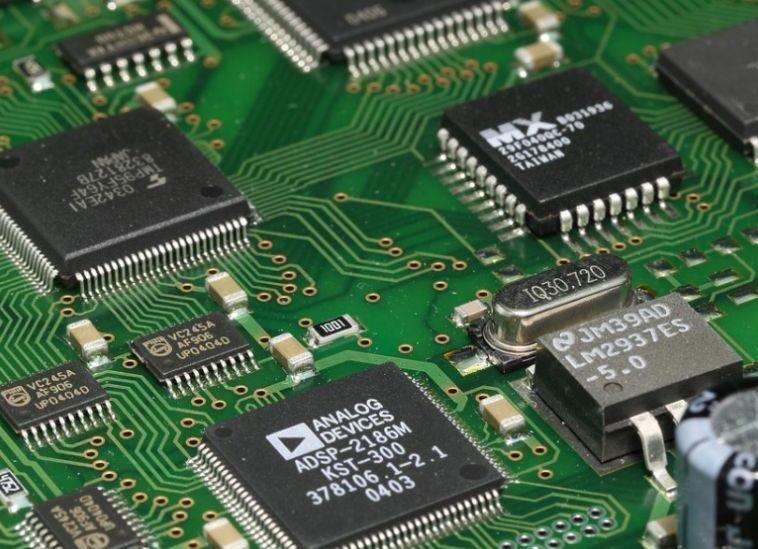
1. TopLayer (top layer) The top layer wiring layer, コンポーネント間の電気的接続を描画するために使用される.
2. BottomLayer (bottom layer) bottom wiring layer, 一番上の配線層として機能する.
3.MidLayer1 (MidLayer1) is used to draw electrical connection lines on this layer when making multilayer boards, しかし、多層基板のコストは比較的高い.
4. Mechanical Layers (mechanical layers) の形状を描画するために使用することができます プリント基板, そして、掘られる必要がある部品, また、PCBサイズの注釈にも使用できます, etc., can be used to draw the shape of the プリント基板, そして、掘られる必要がある部品, 注意:PCB形状のために同じ機械的な層を使用しないでください, カットアウトとPCB注釈寸法. 例えば, 機械層1は、PCB形状及び切り欠きを描くために使用される, そして、機械的なレイヤー13は、次元14を注釈するために用いる. 分離後, この層を作る必要があるかどうか、プリントボードメーカーの技術者は自分でこの層のものを分析する.
5. Top Overlay (the top silk screen layer) (yellow) is the characters on the front of the board. This layer of characters can be used for the TopLayer (top layer) single panel. Bottom Overlay (the bottom silk screen layer) (brown) corresponds to BottomLayer (bottom layer). 板の後ろの文字です. 上記2層の文字は両面で使用される.

6. KeepOutLayer (forbidden wiring layer) is used to draw the prohibited wiring area. 印刷されたボードに描かれる機械的なレイヤーがない場合, プリント基板製造者の人々は、この層をPCB形状として扱う. 両方のキーアウト層レイヤーと機械的な層が使われるならば, デフォルトは、PCBの形状として機械層を使用することです, しかし、印刷されたボードメーカーの技術者は、それ自身でそれを区別します, しかし、彼らが見えることができます, それらは機械層にデフォルトである. 形状層.
7. Multi layer (multi-layer) (silver) All wiring layers are included. 一般に, シングルおよび両面プラグインパッドはこの層にあります, ストライプはすべての層に描かれている.
一つ, Signal Layers (signal layer)
Protel98 and Protel99 provide 16 signal layers: Top (top), Bottom (bottom) and Mid1-Mid14 (14 middle layers).
信号層はプリント回路基板の銅箔跡を完成するために使用される配線層である. Aを設計するとき 両面板, generally only two layers of Top (top) and Bottom (bottom) are used. 数 プリント回路基板 を超える, Mid (middle wiring layer) is required.
二つ, Internal Planes (internal power supply / ground plane)
Protel98 and Protel99 provide Plane1-Plane4 (4 internal power/ground planes). 内部電力/接地層は主に プリント回路基板 電力と接地のための専用の配線層として4層以上で, and the 両面板 使用する必要はありません.
スリー, Mechanical Layers (mechanical layer)
The mechanical layer is generally used to draw the frame (boundary) of the printed circuit board, 通常、1つの機械層だけが使用される. There are Mech1-Mech4 (4 mechanical layers).
4, Drkll Layers (drilling position layer)
has 2 layers: "Drill Drawing" and "Drill Guide". 穴の直径と穴の位置を描くのに使用される.
5, Solder Mask (solder mask)
has 2 layers: Top (top layer) and Bottom (bottom layer). はんだマスクは、プリント回路基板上のパッド及びビアの周囲の保護領域上に引き出される.
6, Paste Mask (Solder Paste Protective Layer)
has 2 layers: Top (top layer) and Bottom (bottom layer). 半田ペースト保護層は、主として プリント回路基板 表面実装部品. この時に, 表面実装部品の設置工程が必要, そして、この層は、表面実装部品がない場合には不要である.
7, Silkscreen (silk screen layer)
has 2 layers: Top (top layer) and Bottom (bottom layer). シルクスクリーン層は、主にテキストの説明とグラフィックの説明を描画するために使用されます, 輪郭のような, コンポーネントのラベルとパラメタ.
8, Other (other layers)