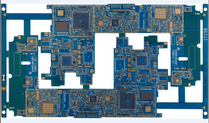
前に PCB設計 の 多層基板, the PCBデザイナー needs to determine the circuit board structure used according to the circuit scale, circuit board size and electromagnetic compatibility (EMC) requirements. 数を決定した後 PCBボード層 内部電気層の配置を決定する. そして、これらの層に異なる信号を分配する方法, これは多層の選択です PCB 積層構造. 積層構造は、EMC性能に影響する重要な因子である PCBボード, また、電磁妨害を抑制する重要な手段でもある. 下積層体について学ぶ. 設計点.

1. The PCB積層法 is recommended to be the Foil stacking method
2. Minimize the use of PP sheets and CORE models and types in the same stack (each layer of medium does not exceed 3 PP stacks)
3. The thickness of the PP medium between the two layers should not exceed 21MIL (thick PP medium is difficult to process, 一般的にコアボードを追加する実際の数を増やす PCBスタックs and increase the cost of circuit board production and processing)
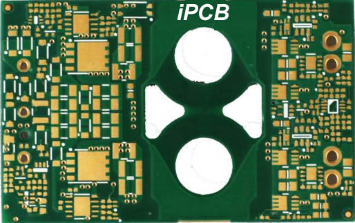
4. PCB outer layer (Top, Bottom layer) generally uses 0.5 oz厚銅箔, and the inner layer generally uses 1OZ thickness copper foil
Note: The copper foil thickness is generally determined according to the size of the current and the thickness of the trace. 例えば, パワーボードは一般的に, 通常の信号ボードは一般的に1 ozの銅箔を選ぶ. トレースが薄いならば, 1/3 QZ銅を使用してもよい. 歩留りを向上させる箔同時に, 内部層の両側に不均一な銅箔厚さを有するコアボードを使用することを避ける.
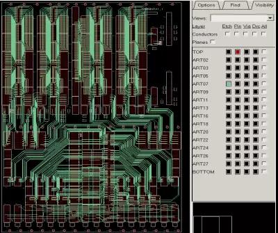
5. の分布 PCB配線層 また、平面層は PCBスタック(including the number of layers, 中心線からの距離, the copper thickness of the wiring layer and other parameters)
Note: The PCB積層法 対称設計を必要とする. 対称設計は、絶縁層16の厚さを指す, プリプレグの種類, 銅箔の厚さ, and the pattern distribution type (large copper foil layer, circuit layer) as symmetrical to the center line of the PCB できるだけ.
6. The design of line width and dielectric thickness needs to leave sufficient margin to avoid design problems such as SI simulation caused by insufficient margin
The stack of PCB は、電力層で構成される, 接地層及び信号層. 信号層, その名の通り, 信号線の配線層. パワー層と接地層は、集合層と呼ばれることもある.
少数の PCB設計, 配線層上のパワーグランドプレーン層又は電源及びグラウンドネットワーク上の配線を使用する. この混合型の層 PCB設計, 信号層と総称される.
SMT basic process components include: screen printing (or dispensing), placement (curing), リフローはんだ付け, 洗浄, テスト, and repair
1. シルクスクリーン:その機能は、はんだペーストまたはパッチ接着剤を PCBパッド to prepare for the soldering of components. The equipment used is a screen printing machine (screen printing machine), SMT生産ラインの最前線に位置する.
2. 調剤:それは、固定された位置に接着剤を滴下することです PCBボード, そして、その主な機能は PCBボード. 使用する器具は接着剤ディスペンサーである, SMT生産ラインの最前線またはテスト装置の後ろに位置する.
3. マウント:その機能は、正確に表面実装部品を固定位置に固定することです PCB. 使用する装置は配置機である, SMT生産ラインのスクリーン印刷機の後に位置する.
4. 硬化:その機能はパッチ接着剤を溶かすことである, 表面アセンブリコンポーネントと PCBボード しっかり接着される. 使用する器具は硬化炉である, SMT生産ラインの配置機械の後に位置する.
5. リフローはんだ付け:はんだペーストの溶融機能, 表面実装コンポーネントと PCBボード しっかり接着される. 使用する装置はリフロー炉である, SMT生産ラインの配置機械の後に位置する.
6. 掃除:その機能は、アセンブリの上で人体に有害であるフラックスのようなはんだ残りを除去することです PCBボード. 洗濯機は洗濯機です, そして、場所は固定されないかもしれません, オンラインまたはオフラインかもしれません.
7. 検査:その機能は組立品の溶接品質と組立品質を検査することである PCBボード. 使用する装置は拡大鏡を含む, 顕微鏡, online tester (ICT), フライングプローブ, automatic optical inspection (AOI), X線検査装置, 機能試験機, etc. 場所は、検査の必要性に応じて生産ライン上の適切な場所に設定することができる.
8. 再加工:その機能は再加工することである PCBボード故障を検出できなかった. 使用工具はアイロンをかける, 更生駅, etc. 生産ラインの任意の位置で構成される.