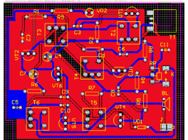
PCB生産プロセスの完全版
今日のあなたの完全なバージョンをもたらします PCB 製造工程, 私は、あなたがより深い理解を持つことができることを望みます PCB 生産!
PCB--Cut Lamination
Objective: according to the requirements of the engineering data M私, the large sheet meeting the requirements is cut into small pieces of production sheet and small pieces to meet the requirements of customers
プロセス: large board cutting according to MI requirements
PCB--Drill hole
Objective: according to the engineering data, drill the required hole diameter at the corresponding position on the plate with the required size
Process: lamination - put on board - drilling - put off board - inspection / 修理
PCB--PTH
Objective: to deposit a thin layer of copper on the wall of insulating hole by chemical method
Process: rough grinding - hanging plate - automatic copper sinking line - lower plate - dilute H2SO4 - increase copper
PCB--Dry film
Objective: graphic transfer is to transfer the image on the production 板へのフィルム
Process: (solder mask process): board grinding - printing the first side - drying - printing the second side - drying - exposure - developing - inspectionï¼ Dry film process: pressing film - standing - alignment - exposure - standing - developing - inspectionï¼
PCB--Etching
Objective: etching is to use chemical reaction method to remove the copper layer of non circuit parts
PCB--Solder mask
Objective: solder mask is to transfer the graphics of green ink, film to the board, so as to protect the circuit and prevent the tin on the circuit when welding parts
Process: grinding plate - printing photosensitive green oil - curium plate - exposure - development; board grinding - printing the first side - drying plate - printing the second side - drying plate
PCB--Silk screen
Objective: silk screen is a kind of mark which is easy to identify
Process: solder mask after final curium - cooling and standing - screen adjustment - character printing - back curium
PCB--Surface treament
Objective: to coat a nickel / プラグフィンガーに必要な厚さの金層, so as to make it have more hardness and wear resistance
Process: grinding board - degreasing - twice water washing - micro erosion - twice water washing - pickling - copper plating - water washing - nickel board - washing - gold plating
PCB--Outline
Objective: through the mold stamping or CNC ゴング machine gongs out of the customer needs the shape forming method, オーガニックゴング, ビアボード, gongs, hand cut
Note: the accuracy of data gong machine board and beer board is higher than that of hand Gong, そして、ハンドカッティングボードはいくつかの簡単な形を作ることができます
PCB--Test
Objective: to detect the open circuit, short circuit and other defects that are difficult to find by visual inspection
Process: mold loading - board setting - test - qualified - FQC visual inspection - unqualified - repair - return to test - OK - reject - scrap
PCB--Final inspection
Objective: through 100% visual inspection of plate appearance defects, マイナー欠陥を修復, to avoid problems and defective plate outflow
Specific work process: incoming materials - check data - visual inspection - qualified - FQA spot check - qualified - packaging - unqualified - treatment - check -OK
So, 上記の完全なプロセスについてです PCB, 他に何か提案があれば, IPCB ようこそあなたと通信する.

PCBプロセス