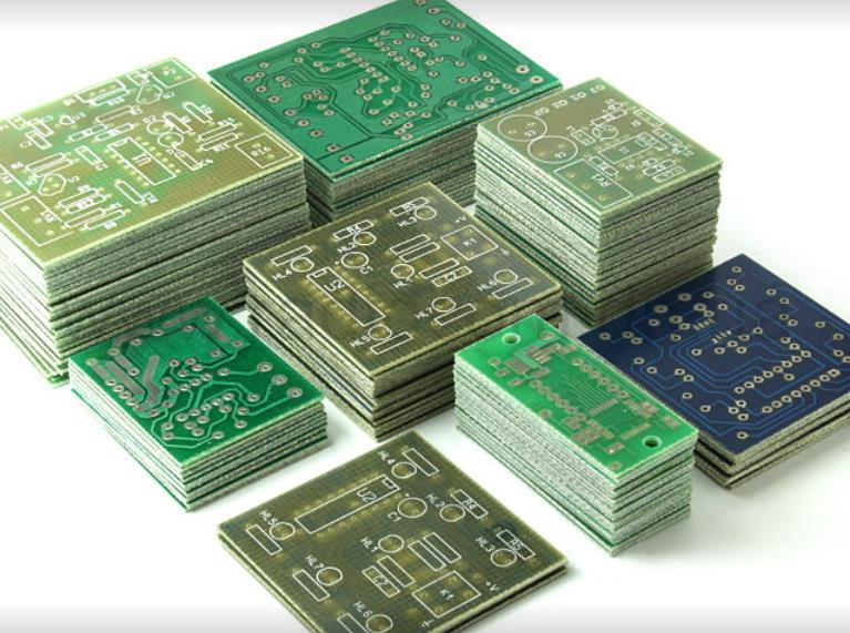
隨著當前可擕式產品的設計向小型化和高密度方向發展, PCB設計 變得越來越困難, 對系統提出了更高的要求 PCB生產 過程. 在當前大多數可擕式產品中, 間距小於0的BGA封裝.65mm採用盲孔和埋孔的設計過程. 那麼什麼是盲人和被埋者?
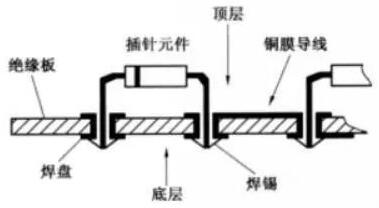
Blind vias (Blind vias / Laser Vias): Blind vias are vias that connect the inner traces of the PCB to the traces on the surface of the PCB. 這個孔沒有穿透整個電路板.
埋入過孔:埋入過孔是僅連接內層之間痕迹的過孔類型, 囙此,它們從PCB表面看不見.
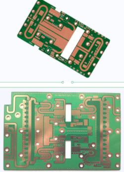
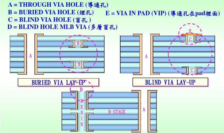
一 8層板:
A: Through hole (L1.-L8)
B: Buried hole (L2.-L7)
C: Blind hole (L7L8)
D: Blind hole (L1-L3)
2 Setting of blind and 埋入過孔
Set Via type:
Click Setup-Pad Stacks in the menu, 然後在焊盤堆棧類型中選擇Via選項, 將出現如右側所示的設定對話方塊.
按一下左下角的添加過孔按鈕,設定所需的過孔類型, 包括鑽孔尺寸, 各層外徑尺寸等參數.
如果是通孔類型, 在左下角的過孔選項中選擇“通過”, 如果是盲埋通孔類型, select the Partial option
When selecting a Partial type via, 必須指定其開始層和結束層. 例如, the blind and buried vias of the V12 and V27 types are set as shown in the figure below

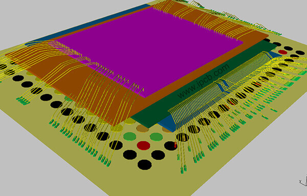
3 PCB電路板製造 process: blind and buried vias
When it comes to blind/buried vias, 我們從傳統的多層板開始. 標準的結構 多層板 包含內部和外部電路. 鑽孔和孔中的金屬化過程用於實現每層電路的內部連接功能. 然而, 因為電路密度的新增, 零件的包裝方法不斷更新.
為了允許有限的PCB區域放置更多高性能零件, 除了較薄的電路寬度之外, 孔徑也從DIP插孔孔徑中的1 mm减小到0.SMD中為6 mm, 並進一步降低到0.4mm或以下. 但它仍然佔據了表面積, 所以有埋洞和盲孔, which are defined as follows:
A. Buried Via
The through holes between the inner layers cannot be seen after pressing, so there is no need to occupy the area of the outer layer
B. Blind Via
Applied to the connection between the surface layer and one or more inner layers.
1. Buried hole design and production
The production process of buried vias is more complicated than that of traditional multilayer boards, 而且成本更高. 通常規定了埋入過孔、一般通孔和焊盤尺寸.
2. Blind hole design and production
The board with extremely high density, 雙面貼片設計, 外層會上下浮動, 和I/O過孔會相互干擾, especially when there is a VIP (Via-in-pad) design, 更麻煩的是. 盲孔可以解决這個問題.