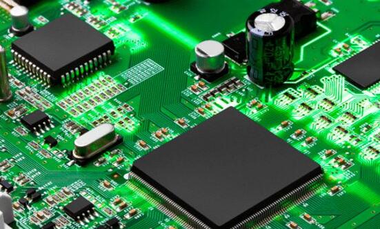
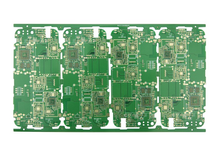
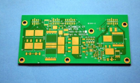
將軍 PCB設計 process is as follows: preliminary preparation -> PCB structure design -> PCB layout -> wiring -> wiring optimization and silk printing -> network and DRC inspection and structure inspection -> plate making.
第一:前期準備. 這包括準備元件庫和示意圖. “如果你想做好, 你必須先把工具磨快.“做一個好的董事會, 除了設計原則之外, 你也必須畫好. 繼續之前 PCB設計, 我們必須首先準備原理圖SCH的元件庫和PCB的元件庫. 組件庫可以使用Peotel自己的庫, 但通常很難找到合適的. 最好根據所選設備的標準尺寸數據創建自己的組件庫. 原則上, 先做PCB元件庫, 然後執行SCH組件庫. PCB組件庫要求很高, 直接影響板的安裝; SCH組件庫要求相對寬鬆, 只要注意引脚内容的定義以及與PCB元件的對應關係. PS:注意標準庫中的隱藏管脚. 然後是原理圖的設計, 當它完成時, 它已準備好啟動 PCB設計.
第二:PCB結構設計. 在此步驟中, 在中繪製PCB表面 PCB設計 根據確定的環境 PCB板 尺寸和各種機械定位, 並放置所需的連接器, 按鈕/開關, 螺釘孔, 裝配孔, 等. 根據定位要求. And fully consider and determine 這個 wiring area and non-wiring area (such as how much area around the screw hole belongs to the non-wiring area).
第3:PCB佈局. 坦率地說, 佈局是將設備放置在電路板上. 此時, 如果上述所有準備工作都完成了, you can generate the netlist (Design->Create Netlist) on the schematic diagram, and then import the netlist (Design->Load Nets) on the PCB圖. 你可以看到整個設備堆棧崩潰, 針腳之間有飛線表示連接. 然後你可以佈置設備. The general layout is carried out according to the following principles:
1 . 根據電力效能的合理劃分, it is generally divided into: digital circuit area (那就是, afraid of interference and interference), analog circuit area (fear of interference), power drive area (interference source);
2 . 完成相同功能的電路應盡可能靠近, 應調整每個組件,以確保最簡潔的連接; 同時, adjust the relative position between the functional blocks to make the connection between the functional blocks the most concise;
3 . 用於高品質部件, 應考慮安裝位置和安裝强度; 加熱部件應與溫度敏感部件分開放置, and thermal convection measures should be considered when necessary;
4 . I/O drive device is as close as possible to the edge of the printed board and to the lead-out connector;
5. . The clock generator (such as crystal oscillator or clock oscillator) should be as close as possible to the device that uses the clock;
6. . 每個集成電路的電源輸入引脚與接地之間, a decoupling capacitor (generally a monolithic capacitor with good high-frequency performance is used); when the board space is dense, 還可以在幾個集成電路鉭電容器周圍添加一個.
7 . A discharge diode should be added to the relay coil (1N4148. is sufficient);
8. . 佈局要求應平衡, 密集有序, not top-heavy or heavy

--Special attention is needed. 放置組件時, the actual size of the components (occupied area and height) and the relative position between the components must be considered to ensure the electrical performance of the circuit board and the feasibility of production and installation 同時 as convenience, 應在確保上述原則能够得到體現的前提下,對組件的放置進行適當修改,使其整潔美觀. 例如, 相同的部件應整齊地放置在同一方向上.
這一步與電路板的整體影像和下一步佈線的難度有關, 囙此,必須考慮一點努力. 佈局時, 您可以進行初步佈線,並充分考慮不確定的地方.
第四:接線. 佈線是整個過程中最重要的過程 PCB設計. 這將直接影響 PCB板. 正在進行中 PCB設計, 接線通常有3個部分:第一, 佈局是最基本的要求 PCB設計. 如果線路沒有連接,到處都是飛線, 這將是一個不符合標準的董事會, 可以說你還沒有開始. 二是對電力效能的滿意度. 這是衡量印刷電路板是否合格的名額. 這是在部署之後, 仔細調整接線, 使其達到最佳電力效能. 然後是美學. 如果您的接線正確部署, 不會影響電器的效能, 但乍一看, 它淩亂多彩, 那麼不管你的電力效能有多好, 在別人眼裡,它仍然是一堆垃圾. 這給測試和維護帶來了極大的不便. 接線應整齊一致, 沒有交叉和無序. 所有這些都必須在確保電器效能和滿足其他個人要求的同時實現, 否則這一天就結束了. The wiring is mainly carried out according to the following principles:
1. . 在正常情况下, 電源線和地線應首先接線,以確保電路板的電力效能. 在條件允許的範圍內, 儘量加寬電源線和地線的寬度, 優選地,地線比電源線寬, their relationship is: ground line>power line>signal line, 通常訊號線寬:0.2 ~ 0.3毫米, 最小寬度可以達到0.050.07毫米, 電源線一般為1.22.5毫米. 用於數位電路的PCB, 可以使用較寬的接地線形成回路, that is, to form a ground net to use (the ground of the analog circuit cannot be used in this way)
2. . Wire the 線 with strict requirements (such as high-frequency lines) in advance, 輸入端和輸出端的邊緣線應避免相鄰平行,以避免反射干擾. 如有必要, 應新增地線進行隔離, 相鄰兩層的佈線應相互垂直. 寄生耦合很容易並行發生.
3. . 振盪器外殼接地, 時鐘線應該盡可能短, 不應該到處都畫. 時鐘振盪電路下, 應擴大專用高速邏輯電路的面積, and other signal lines should not be used to make the surrounding electric field approach zero;
4. . 盡可能使用45º多段線佈線, and 90º polyline should not be used to reduce the radiation of high-frequency signals; (the lines with high requirements should also use double-curved lines)
5. . 不要在任何訊號線上形成回路. 如果不可避免, the loop should be as small as possible; the signal lineâs vias should be as few as possible;
6. . 關鍵線應盡可能短和粗, 兩側加保護地.
7. . 通過扁平電纜傳輸敏感訊號和雜訊場帶訊號時, 它們應以“地線訊號地線”的管道引出.
8. . Key signals should be reserved for testing points to facilitate production and maintenance testing
9. . 原理圖接線完成後, 佈線應優化; 同時, 初步網絡檢查和DRC檢查正確後, 放線區域充滿地線, 並且使用大面積的銅層作為地線. 所有使用的地方都作為地線接地. 也可以製成多層板, 電源線和地線各占一層.
5.PCB佈線工藝要求
1. . String
In general, 訊號線寬為0.3mm (12mil), 電源線寬度為0.77mm (30mil) or 1.27毫米 (50mil); the distance between the line and the line and the pad is greater than or equal to 0.33mm (13mil) ). 在實際應用中, increase the distance when conditions permit;
When the wiring density is high, you can consider (but not recommend) to use two lines between IC pins, 線寬為0.254mm (10mil), 且行距不小於0.254mm (10mil). 在特殊情况下, 當器件引脚密集且寬度較窄時, 可以適當减小線寬和行距.
2. . Pad (PAD)
The basic requirements for pads (PAD) and transition holes (VIA) are: the diameter of the disk is greater than the diameter of the hole by 0.6毫米; 例如, 通用引脚電阻器, 電容器和集成電路, 等., 使用磁片/孔尺寸1.6mm/0.8 mm (63mil/32mil), 插座, 引脚和二極體1N4007, 等., 採用1.8mm/1.0毫米 (71mil/39mil). 在實際應用中, 應根據實際部件的尺寸確定. 如果條件允許, the pad size can be appropriately increased;
The component mounting aperture designed on the PCB板 應為0左右.20.比元件銷的實際尺寸大4mm.
3. . Via (VIA)
Generally 1.27mm/0.7mm (50mil/28mil);
When the wiring density is high, 通孔尺寸可以適當减小, 但它不應該太小, 考慮使用1.0mm/0.6mm (40mil/24mil).
4. . 襯墊的間距要求, lines, and vias
PAD and VIA: 0.3mm (12mil)
PAD and PAD: 0.3mm (12mil)
PAD and TRACK: 0.3mm (12mil)
TRACK and TRACK: 0.3mm (12mil)
When the density is higher:
PAD and VIA: 0.254mm (10mil)
PAD and PAD: 0.254mm (10mil)
PAD and TRACK: 0.254mm (10mil)
TRACK and TRACK: 0.254mm (10mil)
6: Wiring optimization and silk screen printing. “沒有最好的, “只會更好”! 無論你如何刻意設計, 等你畫完, 然後看看, 你仍然會認為許多地方可以修改. 一般的設計經驗是:優化佈線的時間是第一次佈線的兩倍. 在感覺沒有什麼可以修改之後, you can lay the copper (Place->polygon Plane). The copper is generally grounded (note the separation of analog ground and digital ground), 多層板也可能需要電源. 說到絲網印刷, 小心不要被設備堵塞或被過孔和焊盤移除. At the same time, 設計時面朝組件表面, 底層的文字應該鏡像以避免混淆.
7:網絡和DRC檢查和結構檢查. 首先, 在電路原理圖設計正確的前提下, the generated PCB network file and the schematic network file are physically connected to the network check (NETCHECK), and the design is revised in time according to the output file result to ensure the wiring The correctness of the connection;
After the network check is passed correctly, the PCB設計 已檢查DRC, 並根據輸出檔案結果及時修改設計,確保PCB佈線的電力效能. 最後, 需要進一步檢查和確認 PCB板.
8:製版。 在此之前,最好有一個審查過程。
PCB設計是一項發人深省的工作。 任何有思想和經驗的人都應該設計一個電路板。 囙此,在設計時一定要非常小心,充分考慮各種因素(例如,易於維護和檢查,許多人沒有考慮),並不斷改進,你將能够設計出一個好的板。