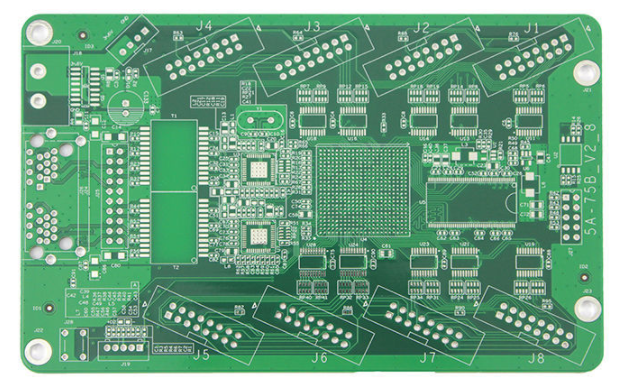
對於不同的應用程序,輸出Gerber檔案的數量不同 PCB設計, 特別是對於 PCB設計 不同層的. 但總的來說, 需要輸出七種類型的電路板數據. These are:

(1)Routing (silk screen layer): If it is more than two layers, 它將分為上, lower or middle routing layer
(2) Silkscreen (silk screen layer): The multilayer board has upper and lower layers. 如果底層沒有絲印, it does not need to be printed;
(3) Plane (power supply, ground plane layer): only for multi-layer boards (output with negative film);
(4) Paste Mask (SMD patch layer);
Mainly for SMD components on PCB板. If all Dip (through hole) components are placed on the board, 無需在此層上匯出Gerber檔案. 將SMD組件連接到 PCB板, 每個SMD焊盤上都必須塗上焊膏. 用於鍍錫的鋼網必須使用粘貼掩模檔案, 可以對膠片進行加工.
粘貼掩模層的Gerber輸出最重要的一點是要清楚, 那就是, 該層主要用於SMD組件. 同時, 將該層與下麵將介紹的焊接掩模進行比較,找出兩者的不同功能, 因為從電影圖片上看,這兩張電影圖片非常相似.
(5) Solder Mask (main welding layer);
The main purpose is to ensure that the selected options (such as component foot pads and some special copper skins, 等.) are not covered by green oil on the PCB板 並以銅皮的形式直接出現在電路板上. 所有需要焊接和粘貼的物體都沒有被綠油覆蓋. 必須選擇它. 簡單地說, 如果你想在設計中以裸銅的形式出現在電路板上, 您可以在輸出主焊料層中選擇它.
對於主焊料層Gerber, 必須選擇輸出選項Pads, but the Pads (component foot pads) of the main solder layer are different from PastMask. 它包括SMD和Dip焊盤, 但PastMask僅包含 SMD焊盤.
(6) NC Drill (NC drilling layer);
For the PCB板設計 with through holes, 數控鑽輸出檔案必不可少. 沒有此檔案, 不可能在 PCB板.
(7) Drill Drawing (drilling reference layer);
The drilling reference chart is a data reference chart provided for drilling. 注意這一層的輸出. 設定選項時, 通常需要選擇具有鑽孔的對象, 因為其輸出主要用於鑽孔對象, such as Pads (pads) and Vias (vias).
Summarize:
When outputting film files, 它通常基於這七個類別. 您只需要根據此標準輸出. 需要輸出多少膠片檔案取決於設計的PCB. 例如, 單個面板沒有底部接線和平面. (Plane) layer, 但可能有兩個絲網蓋伯檔案, 等., 多層板上可能有兩個以上的佈線層. 只要輸出Gerber檔案的概念清楚, 不管設計有多複雜, 它永遠不會與它分離.