中的常見錯誤 schematic diagrams:
(1) 這個re is no signal connected to the ERC report pin:
a. 我/O attributes are defined for the pins when the package is created;
b. 創建或放置組件時,會修改不一致的網格内容, and the pins and wires are not connected;
c. 創建零部件時, 銷方向相反, 必須連接非pin名稱端.
(2) The component went out of the drawing boundary: no component was created in the center of the diagram paper of the component library.
(3.) The network table of the created project file can only be partially imported into the PCB: when the netlist is generated, 未選擇全域.
(4) When using multi-part components created by yourself, 從不使用注釋.

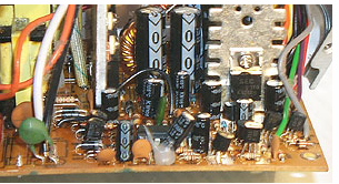
2. Common errors in PCB板:
(1) It is reported that NODE is not found when loading the network:
a. The components in the schematic diagram use packages that are not in the PCB library;
b. The components in the schematic diagram use packages with inconsistent names in the PCB library;
c. 原理圖中的元件使用PCB庫中引脚編號不一致的封裝. 例如, 3極管:sch中的管脚號為e, b, c, PCB中的管脚編號為1, 2, 3.
(2) It is always impossible to print on one page when printing:
a. It is not at the origin when creating the PCB library;
b. 組件已移動和旋轉多次, 還有隱藏的字元在 PCB板. 選擇顯示所有隱藏字元, 收縮PCB, 然後將角色移動到邊界.
(3) The DRC reporting network is divided into several parts:
在裡面dicates that this network is not connected. 查看報告檔案並使用連接的銅纜查找它.
此外, 提醒朋友儘量使用WIN2000,减少藍屏的機會; 多次匯出檔案以生成新的DDB檔案,以减少文件大小和PROTEL凍結的機會. 如果你做一個更複雜的設計, 儘量不要使用自動路由.
In PCB設計, 佈線是完成產品設計的重要步驟. 可以說,之前的準備工作已經做好了. 在整個PCB中, 佈線設計過程具有最高限制, 最優秀的技能, 工作量最大. PCB佈線 包括單面佈線, 雙面佈線和多層佈線. 還有兩種接線管道:自動接線和互動接線. 自動接線前, 您可以使用interactive預先連接要求更高的線路. 輸入端和輸出端的邊緣應避免相鄰和平行,以避免反射干擾. 如有必要, 應新增地線進行隔離, 相鄰兩層的佈線應相互垂直. 寄生耦合很容易並行發生.
自動佈線的佈線率取決於良好的佈局。 可以預設佈線規則,包括彎曲次數、過孔數和步驟數。 通常,首先探索扭曲佈線,快速連接短線,然後執行迷宮佈線。 首先,針對全域佈線路徑優化要鋪設的佈線。 它可以根據需要斷開鋪設的電線。 並嘗試重新佈線,以提高整體效果。
當前的高密度 PCB設計 感覺通孔不合適, 而且浪費了很多寶貴的佈線通道. 為了解决這一衝突, 出現了盲孔和埋孔科技, 這不僅實現了通孔的作用,還節省了大量的佈線通道,使佈線過程更加方便, 更平滑, 更完整. The PCB板 設計過程是一個複雜而簡單的過程. 好好掌握它, 需要大量的電子工程設計. 只有當員工親身體驗時,他們才能獲得它的真正含義.