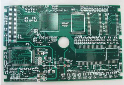
PCB電路板 生產過程和 PCB製造 process
The inventor of the printed circuit board was Paul Eisler, 奧地利人, 1.936年,誰在無線電設備中使用了印刷電路板. 1943年, 美國人在軍用無線電中廣泛使用了這項科技. 1948年, 美國正式承認這項發明用於商業用途. 自20世紀50年代中期以來, 印刷電路板科技才剛剛開始被廣泛採用.

在印刷電路板出現之前, 電子元件之間的互連是通過直接連接實現的. 但是現在, 電路板只是一種有效的實驗工具; 印刷電路板在電子工業中佔據絕對主導地位.
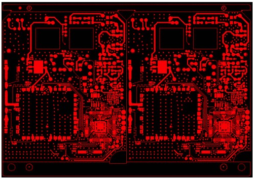
1. Detailed explanation of relevant design parameters:
one. line
1. Minimum line width: 6mil (0.153mm). 也就是說, 如果線寬小於6mil, 它將無法生產. 如果設計條件允許, 設計越大, 更好, 線寬越大, 工廠越好, 產量越高, 和將軍 PCB設計 例行程式約為10mil. 這是非常重要的, and the design must be consider
2. Minimum line spacing: 6mil (0.153mm). 最小線距為線到線距離, 線路到墊板的距離不小於6mil. 從生產角度來看, 越大越好, 一般規則是10mil. 當然, 如果設計是有條件的, 越大越好. 這是非常重要的. Design Must consider
3. 直線和輪廓線之間的距離為0.508mm (20mil)
two. via via (commonly known as conductive hole)
1. 最小孔徑:0.3mm (12mil)
2. The minimum via hole (VIA) aperture is not less than 0.3mm (12mil), and the single side of the pad cannot be less than 6mil (0.153mm), 最好大於8mil (0.2mm), but not limited (see Figure 3) 這一點非常重要, The design must be considered
3. The via hole (VIA) hole-to-hole spacing (hole side to hole side) cannot be less than: 6mil, preferably greater than 8mil. This point is very important, and the design must be considered
4. 焊盤和輪廓線之間的距離為0.508mm (20mil
Third, the production process
Double-sided tin plate/immersion gold plate production process: cutting-drilling--sinking copper-circuit-drawing electricity-etching-solder mask ---Character----Spray tin (or heavy gold)-Gong edge-V cut (some boards donât need)-----Fly test----Vacuum packaging
Multi-layer tin board/immersion gold board production process: cutting-inner layer--lamination-drilling--sinking copper-circuit--map electricity- ---Etching-----Solder Mask---Character----Spray Tin (or Immersion Gold)-Gong Edge-V Cut (Some Boards Not Needed)-----Fly Test---- Vacuum packaging