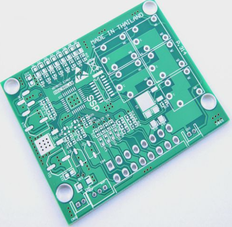
如何優化 PCB佈局 to improve power module performance

The global energy shortage problem has caused governments all over the world to vigorously implement a new energy saving policy. 電子產品的能耗標準越來越嚴格. 供電源設計工程師使用, 如何設計更高效、更高效能的電源是一個永恒的挑戰. 從電源佈局開始 PCB板, 本文介紹了最好的 PCB佈局 方法, 優化簡單開關電源模塊效能的示例和科技.
規劃電源佈局時, 首先要考慮的是兩個開關電流回路的物理回路面積. 雖然這些回路區域在電源模組中基本不可見, 瞭解兩個回路各自的電流路徑仍然很重要,因為它們將延伸到模塊之外. 在圖1所示的迴圈1中, the current self-conducting input bypass capacitor (Cin1) passes through the MOSFET during the continuous on-time of the high-side MOSFET to the internal inductor and output bypass capacitor (CO1), 最後返回輸入旁路電容器.
回路2在內部高側MOSFET的關閉時間和低側MOSFET的開啟時間期間形成. 存儲在內部電感器中的能量流經輸出旁路電容器和低側MOSFET, and finally returns to GND (as shown in Figure 1). The area where the two loops do not overlap each other (including the boundary between the loops) is the high di/dt電流面積. The input bypass capacitor (Cin1) plays a key role in providing high-frequency current to the converter and returning the high-frequency current to its source path.
以上介紹了如何優化 PCB佈局 提高功率模組的效能. Ipcb也提供給 PCB製造商 和PCB製造技術.