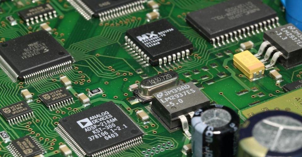
印刷電路板的抗干擾設計與特定電路密切相關. 這裡只有幾項 PCB抗干擾設計
解釋了一些常見的措施.

1. Power cord design
According to the current of the printed circuit board, 儘量新增電源線的寬度,以减少回路電阻. 同時, 製作電源線
, 地線的方向與資料傳輸的方向一致, 這有助於增强抗雜訊能力.
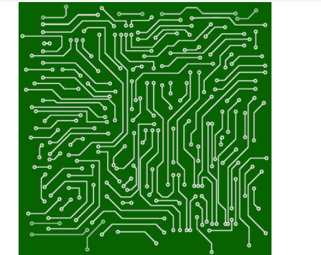
2. Ground wire design
這個 principle of ground wire design is:
1. 數位接地與類比接地分離. 如果上同時存在邏輯電路和線性電路 PCB電路板, 它們應該盡可能地分開
. 低頻電路的接地應盡可能在單點並聯接地. 當實際接線困難時, 它可以部分串聯,然後並聯接地.
The 高頻PCB電路 應在多個串聯點接地, 接地線應短且租用, 高頻分量周圍應盡可能使用網格狀大面積接地箔.
2. 接地線應盡可能厚. 如果地線使用非常細的線路, 接地電位隨電流的變化而變化, so that
The anti-noise performance is reduced. 因此, 接地線應加厚,使其能够通過印製板上允許電流的3倍. 如果可能的話
, 接地線應在2~3mm以上.
3. 接地線形成閉合回路. 僅由數位電路組成的印製板, the grounding
High anti-noise ability.
3. Decoupling capacitor configuration
One of the conventional methods of PCB design is to configure appropriate decoupling capacitors on each key part of the printed circuit board.
The general configuration principle of the decoupling capacitor is:
1. 在電源輸入端連接一個10~100uf的電解電容器. 如果可能的話, 最好連接到100uF或更高.
2. 原則上, 每個集成電路晶片應配備0.01pF陶瓷電容器, 如果印製板的間隙不够,
每4~8片可配置1~10pF電容器.
3. 對於抗雜訊能力弱且關機時功率變化大的設備, 例如RAM和ROM儲存設備, they should be installed in the chip's
Connect the decoupling capacitor directly between the power line and the ground line.
4. 電容器引線不宜過長, 特別是高頻旁路電容器. 此外, the following two points should be noted:
A. 當有接觸器時, 繼電器, 印製板中的按鈕和其他組件. 操作時會產生大量火花放電
, 圖中所示的RC電路必須用於吸收放電電流. 通常地, R為1~2K, C是2.2~47UF.
B、CMOS的輸入阻抗非常高,容易感應,囙此未使用的端子在使用時應接地或連接到正電源。
7. Useful suggestions for using logic circuits: do not use high-speed logic circuits that can be used; add decoupling between the power supply and the ground
Capacitance; pay attention to waveform distortion in long-line transmission; use R-S trigger as a buffer for cooperation between buttons and electronic circuits
Good things to share! 責備, 證據, 歡迎提出建議!