CA.M工程師應注意的13件事 PCB設計
以下內容基本上是每個 PCB製造商, 但它們並不完全相同, 不同的供應商是不同的.
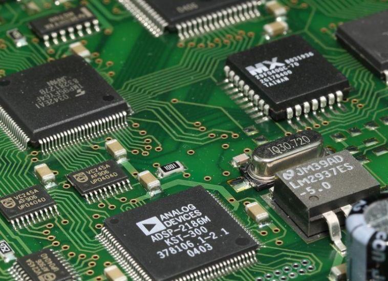
一 土地重疊

The overlap of pads (except surface mount pads), 那就是, 孔的重疊放置, 鑽孔時,由於一個地方有多個孔,會導致鑽頭斷裂和鋼絲損壞.
二. Misuse of the graphics layer
1. 違反常規設計, 例如底層的部件表面設計和頂部的焊接表面設計, 導致檔案編輯時檔案的正面和背面出現錯誤,產品報廢.
2. 如果有槽需要在 PCB板, 使用禁止層或板層繪製它們, do not apply other layers or fill them with pads to avoid mis-milling or miss-milling
3. 如果雙面板上有不需要金屬化的孔, 應單獨說明.
3. Shaped hole
If there are irregular holes in the board, 使用禁止層繪製與孔大小相同的填充區域. 長度/异形孔的寬度比應為–2:3:1, and the width should be >1mm. 否則, 鑽孔機在加工异形孔時容易折斷刀具, 這將導致處理困難.
四. Character placement
1. 字元覆蓋焊盤SMD焊接件, 這給印製板的連續性測試和元件的焊接帶來了不便.
2. 角色設計太小, 這使得絲網印刷困難,字元不够清晰. 字元高度–30mil, 寬度–6mil.
五. Single-sided pad aperture setting
1. 單面襯墊通常不鑽孔. 如果需要標記鑽孔, 孔徑應設計為零. 如果該值設計為在生成鑽井數據時, 將在該位置鑽孔, 這會影響電路板的外觀, 董事會將被廢除.
2. 如果需要鑽孔單面襯墊, 必須做特殊標記.
六. Draw pads with filling blocks
Drawing pads with filler blocks can pass the DRC inspection when designing the circuit, 但這不利於加工. 因此, 類似的焊盤不能直接生成焊接掩模數據. 應用阻焊劑時, 填充塊區域將被阻焊劑覆蓋, 導致設備焊接困難.
七. There are too many filler blocks in the design or the filler blocks are filled with very thin lines
1. 燈光繪圖資料丟失, 燈光繪圖數據不完整, 光繪變形.
2. 因為在光繪資料處理過程中,填充塊是用線逐個繪製的, 生成的光繪數據量相當大, 這新增了資料處理的難度.
八. Surface mount device pad is too short
This is for continuity testing. 對於密度過大的表面貼裝設備, 兩個引脚之間的間距非常小, 而且墊子也很薄. The installation test must be staggered up and down (left and right), 比如墊子設計太小. 短的, 雖然它不影響設備的放置, 但這會使測試銷錯開.
九. The spacing of the large area grid is too small
The edges between the same lines that make up the large-area grid are too small (less than 0.30mm), 這將導致列印過程中短路.
十. The distance between the large area of copper foil and the outer frame is too close
The outer frame of the large area copper foil should be at least 0.相隔20mm, 因為銑削形狀時, 這很容易導致銅箔翹曲,並導致焊劑脫落.
十一. The design of the outline frame is not clear
Some customers have designed contour lines in KEEP LAYER, 電路板層, 頂層, 等. 這些等高線並不重疊, 這使得在成型過程中很難確定哪一條是輪廓線.
十二. Line placement
The line between the two pads, 不要斷斷續續地畫圖, 如果你想加厚界線, 不要使用該線重複放置, 直接更改線寬即可, 囙此,在修改線條時很容易進行修改.
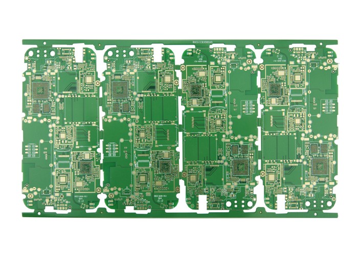
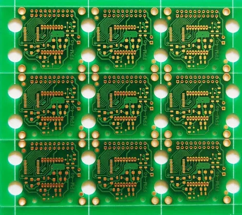
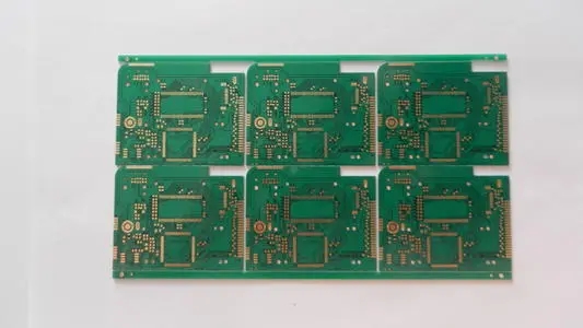
十3. Imposition
The track system of the automatic welding equipment has a size range for clamping the PCB板. The clamping range of the general production line is: 50mm*50mm-460mm*460mm. The small 50mm*50mm PCB板 需要設計成拼版形式.
A. PCB must have its own reference point (Mark) to facilitate the automatic location of welding equipment.
B. 如果採用V形切割處理方法, 施加間距應保持在0.3毫米, 工藝的單面邊緣應為5mm.
C. 對於形狀複雜的PCB, 組裝後的PCB應盡可能確保形狀規則,以便夾持軌道.
D. 相同的PCB可以放在一起, 不同的PCB也可以放在一起.
E. 拼版可以採用平排的形式, 相反行, 或者鴛鴦板.