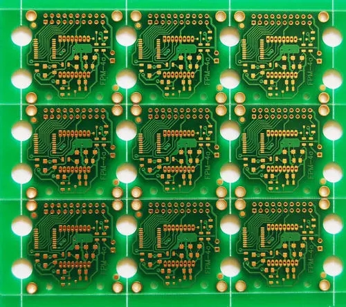
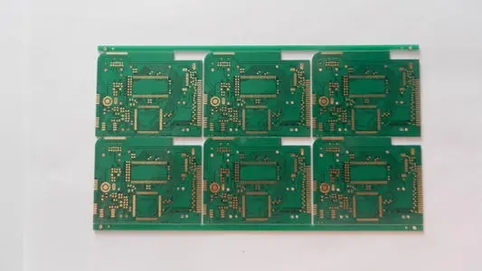
沒有什麼特別的 PCB佈局 之前, 尤其是手機. 一開始, 我覺得什麼都沒有, 但最終, 我真的瘋了. 沒有出路了. 真實的! 老闆開始談論6天. 從佈局開始, 我不知道老闆是不是瘋了. 實際上,一些同事說是的! 我真的很想用菜刀切人. 後來, 老闆說:“有點緊, 否則, 兩個人一起做. 我依靠, 老闆真的很有創意. 沒有辦法叫我兼職. 就像這樣, 我最痛苦和最長的PCB佈局開始了. 此外, 幾天前已經有6周沒有休息了, 現在一切都好了. 晚上上班很酷! 凉的!

現在我真的不想活了!
不要說你做得比做得不好要好, 即使不成功.
別胡說八道了, 讓我先談談我的經歷. 如果有專業人士, 專家或高級工程師, 請給我們更多的意見和建議!
我使用POWER PCB 5.0.
1. The thread ends first
2. Tightly trace
3. 上部和下部導線應盡可能重疊, leaving room for punching holes
4. 佈線時不要堵塞道路, give the surrounding space as much as possible
5. The punching area and wiring area can be separated
6. GND除外, 减少通孔.
7. Less wiring in the lower layer of the IC
8. 熟練使用工具, functions and quick decision keys
9. Do not run wires on the holes
10. 如有必要, holes can be punched on the BGA pads
11. 佈局非常重要, analyze the density and direction of the flying line (the principle of proximity)
12. You can go close to the peripheral devices first (if there is a flying line, 你可以在周邊設備上行走, and try to make as little as possible)
13. 如果有多個連接, 看看附近方便的地方, then go where
14. 在IC下打孔後, it is best to walk closer to the IC boundary
15. 儘量在短期內浮出水面.
16. 接線時, 相應的示意圖, it is best to print it out
17. 首先,在表層上取靠近集成電路的線, 這樣你就可以在那裡打洞了. (No worries)
18. 佈局時, 那些可以放得更近的必須放得更近, 尤其是在BGA周圍, 佈局是第一個, 模式是第二種, 美是第3位.
19. 佈線是一項系統性任務, 最好由一個人完成, 如果不止一個, 它會導致死亡.
20. 如果你能計畫好籃子, 你必須考慮邊際,爭取空間.
21. 製作示意圖時, 它必須簡潔明瞭, 使用更少的組件, 高度集成, 並密封, 小的, 必須拆下可選部件.
22. Distinguish which lines are set or settable (there is no other way to move) should go first, 以後再搬.
23. 如果可能的話, 在佈局期間保留設備之間的軌跡寬度.
24. Three-dimensional lines should be used for large-scale BGA ICs (multi-layers). Do not use flat surfaces (all on the same layer). 稍後你就會知道這意味著什麼.