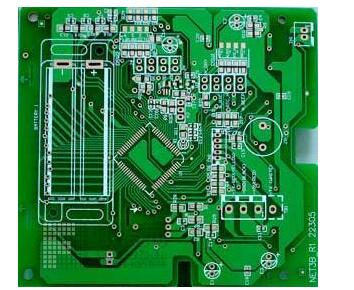
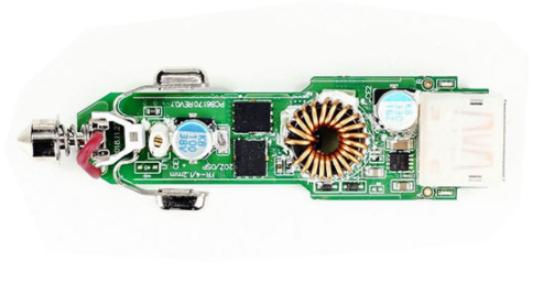
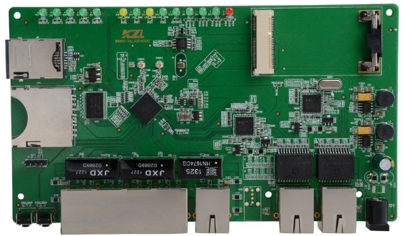
PCB板的PCBA焊接工藝要求
什麼時候 PCBA焊接 已處理, 通常有許多要求 PCBA板, 且板材必須符合要求才能接受焊接加工. 那麼,為什麼焊接工藝需要對電路板有這麼多要求呢? 原來在PCBA加工過程中, 將有許多特殊過程, 特殊工藝的應用立即對PCB板提出了要求. 如果PCB板有問題, 這將新增PCBA焊接過程的難度, 最終可能導致焊接缺陷, 不合格板, 等. 因此, 為了確保特殊工藝的順利完成,方便PCBA焊接工藝, PCB板必須在尺寸和焊盤距離方面滿足可製造性要求. 那麼今天我將向你展示PCBA焊接工藝是如何正確的. PCB板的要求.

1. PCB size
The width of the PCB (including the edge of the board) should be greater than 50mm and less than 460mm, and the length of the PCB (including the edge of the board) should be greater than 50mm. 如果尺寸太小, 它需要做成拼圖.
2. PCB board edge width
Board edge width: >5毫米, panel spacing: <8mm, distance between pad and board edge: >5mm
3. PCB bending
Upward bending degree: <1.2毫米, downward bending degree: <0.5mm, PCB distortion: maximum deformation height ÷ diagonal length <0.25
4、PCB板標記點
標記形狀:標準圓, 廣場, triangle;
Mark size: 0.8~1.5mm;
Mark 材料: gold-plated, 鍍錫的, copper and platinum;
Mark's surface requirements: the surface is flat, 平整的, 未氧化, and free of dirt;
Mark's surrounding requirements: there should be no green oil or other obstacles within 1mm, which is obviously different from the Mark's color;
Mark position: 3mm above the edge of the board, 不應該有像過孔這樣的標記, 測試點, 等. 板周圍5mm以內.
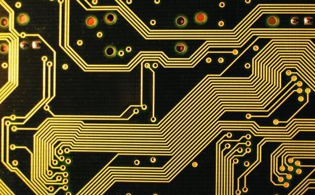
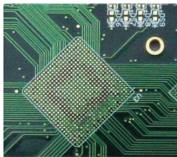
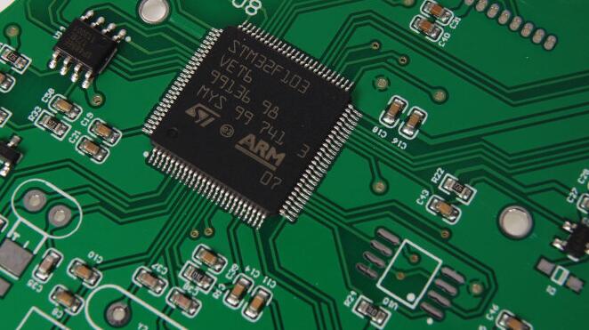
5. PCB pads
There are no through holes on the pads of SMD components. 如果有通孔, 焊膏將流入孔中, 導致設備中的錫更少, 或者鐵罐流到另一邊, 導致板面不平,錫膏無法印刷.
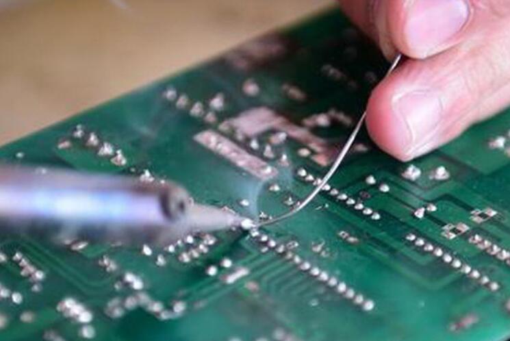
進行時 PCB設計 和生產, 有必要瞭解 PCBA焊接 process, 使產品適合生產. 首先瞭解加工廠的要求可以使後續的製造過程更加順利,避免不必要的麻煩.
這是的要求 PCBA焊接 正在處理 PCB板. 生產時 PCB板, 不要放鬆他們的努力. 只有通過生產高品質且符合要求的產品 PCB板 董事會能否更好地接受其他特殊流程, 賦予PCB板生命,注入功能靈魂. .