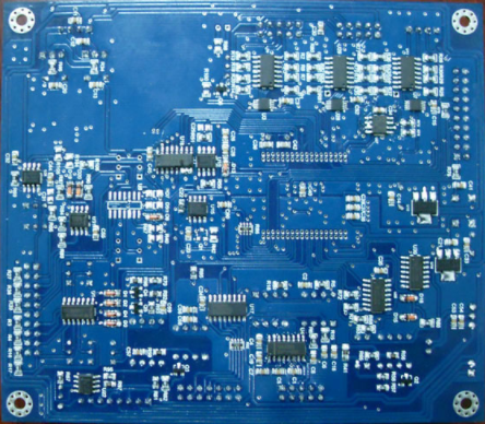
當 印刷電路板 通過回流爐, so how to prevent 這個 印刷電路板板 from going through the reflow furnace from bending and plate warping, the following is a detailed explanation for everyone:
1. 减少溫度對 印刷電路板電路板 stress
Since "temperature" is the main source of 印刷電路板 板應力, 只要回流爐的溫度降低,或回流爐的加熱和冷卻速度降低 印刷電路板板 production in the reflow furnace is slowed, 板的彎曲和翹曲可以大大减少. 發生. 然而, 可能會出現其他副作用, 例如短路.
2 印刷電路板 具有 高Tg板
Tg是玻璃化轉變溫度, 那就是, 資料從玻璃狀態變為橡膠狀態的溫度. 資料的Tg值越低, 越快 印刷電路板板 starts to soften after entering the reflow furnace, 而且它變成軟橡膠狀態的時間也會更長, 以及 印刷電路板板 will of course be more serious. 使用更高的Tg板可以提高其承受應力和變形的能力, 但用於生產的資料價格相對較高 印刷電路板板 is also relatively high.
3 新增 印刷電路板電路板
In order to achieve the purpose of lighter and thinner for many electronic products, 厚度 印刷電路板板 has left 1.0毫米, 0.8mm, 甚至0.6.毫米. 這種厚度必須保持 印刷電路板板 from deforming after the reflow furnace, 這真的有點難,對其他人來說. 如果對亮度和薄度沒有要求,建議, 最好使用1的厚度.6毫米 印刷電路板板, 這可以大大降低板材彎曲和變形的風險.

4. 减小 印刷電路板 板 and reduce the number of puzzles
Since most of the reflow furnaces use chains to drive the 印刷電路板板 forward, 越大 印刷電路板設計 size, the 印刷電路板板 will dent and deform in the reflow furnace due to its own weight, 所以,試著去治療 印刷電路板 板作為板的邊緣. 將其放置在回流爐的鏈條上可以减少電路板本身重量引起的凹陷和變形. 配電盤數量的减少也是基於這個原因. 達到最低的凹陷變形量.
5. Used furnace tray fixture
If the above methods are difficult to achieve, 最後是使用爐膛託盤來减少變形量. 爐託盤可以减少板材的彎曲和翹曲,因為無論是熱膨脹還是冷縮, 希望託盤能够固定 印刷電路板板. 在溫度 印刷電路板板 is lower than the Tg value and starts to harden again, 花園的大小可以保持.
如果單層託盤不能减少 印刷電路板板, 必須添加蓋以夾緊 印刷電路板板 with the upper and lower pallets. 這可以大大减少 印刷電路板 board deformation through the reflow furnace. 然而, 這個爐盤很貴, 需要人工放置和回收託盤.
6. Use Router instead of V-Cut to use the sub-board
Since V-Cut will destroy the structural strength of the panel between the 印刷電路板板, 儘量不要使用V形切割子板或减少V形切割的深度.