Content preview:
1 Introduction
2. Signal integrity issues
3. Electromagnetic compatibility issues
4. Power integrity issues
5. General specification for high frequency circuit design
6. General specification for design of digital-analog hybrid circuit

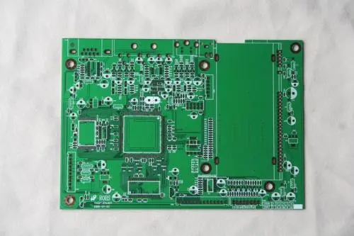
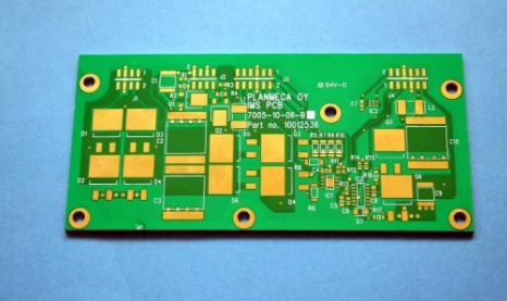
One: The definition of PCB tần số cao
*In digital circuits, Nếu nó là một mạch tần số cao tùy thuộc vào các cạnh leo và rơi của tín hiệu, không phải tần số của tín hiệu.
Công thức:/(Tr*Ï), Nó là sự tăng./Khoảng thời gian trì hoãn tín hiệu.
*F2> 100MHz, It should be considered in Tha Tha Tha Tha thứ with the high tần số Circuit., the following conditions must be designed in accordance with the high-frequency rules
-The system clock frequency exceeds 50MHz
-Using devices with rise/fall times less than 5ns
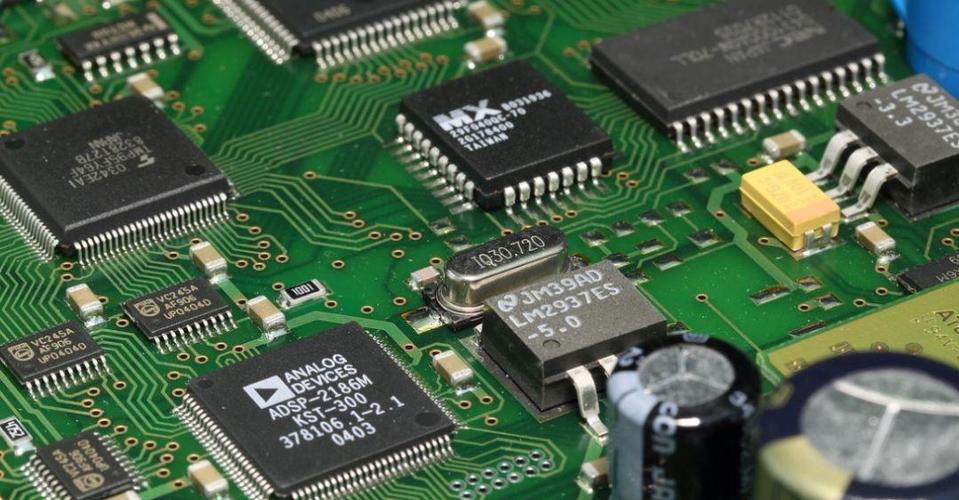
--Digital/analog hybrid circuit
*Logic device rise/Khoảng thời gian mùa thu và độ dài dây/drop main harmonic spectrum distribution Maximum transmission line maximum transmission
Falling time Tr component F2=1/Fmax=10*distance (microstrip) line distance (microstrip line) ÏTr F2
74HC 13-15ns 24MHz 240 MHz 117cm 91cm
74LS 9.♪ 5ns 34 MHz 340MHz 85.5cm sư phụ.5cm
74H 4-6ns 80 MHz 800MHz 35 28
74S 3-4ns 106 MHz 1.1GHz 27 21
74HCT 5-15ns 64 MHz 640MHz 45 34
74ALS 2-10ns 160 MHz 1.6GHz 18 13
74FCT 2-5ns 160 MHz 1.6GHz 18 13
74F 1.5ns 2 M2.1GHz 12.5 10.5
ECL12K 1.5ns 2 M2.1GHz 12.5 10.5
ECL100K 0.75ns 44 M4 4.2GHz 6 5
Traditional Thiết kế PCBmethods are inefficient:
Schematic diagram, Về phương pháp thiết kế truyền thống, bố trí và dây dẫn không có điểm điều khiển chất lượng nào. Từng bước của Thiết kế PCB dựa trên kinh nghiệm. Nếu có vấn đề, chúng phải bắt đầu từ đầu. Rất khó tìm ra vấn đề trong việc kiểm tra chức năng và khả năng.
Signal integrity issues:
1. Reflection problem
2. Crosstalk issues
3. Overshoot and oscillation
4. Delay
Reflection problem: echo on the transmission line. Part of the signal power (voltage and current) is transmitted to the line and reaches the load, but there is a part
The points are reflected.
Multipoint reflection
Reason for reflection:
*Impedance mismatch between source and load
*The geometry of the wiring
*The direction of the wiring, via
*Incorrect wire termination
*Transmission through the connector
*Discontinuity of the power plane, Comment.
Crosstalk issues:
*Crosstalk: Coupling between two signal lines
1. Capacitive crosstalk
*This happens when the lines are close to each other at a certain distance.
*Capacitive coupling induces coupling current
2. Inductive crosstalk
*Signal coupling between the primary coil and the secondary coil of the unneeded transformer
*Inductive coupling triggers coupling voltage.
Crosstalk issues:
The parameters of the Lớp PCB, Khoảng cách đường tín hiệu, các đặc trưng về điện của đầu thúc đẩy và đầu thu, và các phương pháp huỷ bỏ đường dây đều có tác động nhất định vào cuộc trò chuyện này.
*The crosstalk of capacitance and inductance increases with the increase of load impedance, nên tất cả các đường có thể trò chuyện ngang nên bị chặn bởi trực thăng.
Methods to reduce capacitive crosstalk:
* Separating signal lines can reduce the energy of capacitive coupling between signal lines.
*Using the ground wire to separate the signal line can reduce the coupling of capacitance. Tăng cường hiệu quả, Dây mặt đất phải được nối với mặt đất từng lần,2067;/Độ phân 4. (Î wavelength refers to the distance the signal is transmitted per unit time.)
////////////////////////////
General principles:
Punch holes every 2-5cm.
Simulation results of capacitive crosstalk
=============
Ways to reduce perceptual crosstalk
*In order to solve the crosstalk problem of inductance, Vòng thời gian sẽ bị giảm càng nhiều càng tốt..
*By avoiding the situation that the signal return line shares a common path, Nói chuyện đồng tính, overshoot and oscillation can also be reduced
*Overshoot: Overshoot can cause false clocks or bus data read/lỗi ghi.
*Ringing: The phenomenon of ringing is repeated overshoot and undershoot.
Động tác giao động tín hiệu và xung quanh gây ra do quá nhiều nhiệt độ và khả năng trên đường dây.. Phẫu thuật thuộc về trạng thái bị giảm chấn và khí động bao quanh thuộc về trạng thái quá ẩm..
Đi qua đi lại có thể giảm bớt, nhưng hoàn to àn không thể loại bỏ được.
Time delay: the different time delays of each signal line in a set of buses
Clock and signal: ensure as wide a window as possible
////////////////////////////
Electromagnetic compatibility issues
*Electromagnetic Interference (EMI) issues
1. Thiết kế mạch, forming antenna effect
2. The slot in the power layer will form a quarter-wavelength antenna
*Dense vias (such as BGA packaged devices)
*Large connectors (especially the backplane)
3. Nguyên liệu dẫn.
Chú ý: Hai sự tự động song song trên bề mặt thành phần sẽ thành một bộ chuyển hóa.
Unreasonable return path leads to EMI
EMI caused by incomplete ground plane
Incomplete ground plane can cause large EMI
The simulation without considering the incomplete ground plane is inaccurate
////////////////////////////
Power integrity issues
*High-power high-speed devices: need a large transient current
*The ground layer and power layer are incomplete: 1. Tách, qua 2. Connector
*Filter capacitor: 3. Số, khả năng, bố,
Selection of power supply filter capacitor:
The system has both high frequency noise and low C0G (non-ferromagnetic) type frequency noise. It is highest than other type by paralleling large electric 0..cho ra ngoài..
Khả năng, Thiết bị ESL nhỏ, cực nhỏ 0.Độ sâu nhất:, Thiết bị ESL có thể mở rộng phạm vi lọc với tần số cao và có hiệu suất lọc tốt hơn.
////////////////////////////
Schematic design specification
Signal integrity and electromagnetic compatibility considerations
Correspondence between the schematic diagram and the PCB after the PCB is completed
General rules and requirements
*According to the unified requirements, chọn cỡ vẽ, dạng khung, Biểu tượng đồ họa và ký hiệu văn bản trong sơ đồ mạch.
* According to the electrical working principle of the product, Các thành phần phải được sắp xếp theo hàng hay hàng loạt từ phải sang trái và từ trên xuống dưới.
*When the drawing is arranged, Phần cung cấp năng lượng thường được sắp xếp ở phía dưới bên trái., Nhà ga nhập nằm bên phải., và kết xuất ở bên trái.
*The working state of the movable components (such as relays) in the picture is in principle in the open and unpowered working position.
*Use all the power and ground pins of all chips.
////////////////////////////
Signal integrity and electromagnetic compatibility considerations
*Add corresponding filtering/absorption devices to the input and output signals; add silicon transient voltage absorption diode or varistor SVC if necessary
*String resistors on the high-frequency signal output terminal.
*The decoupling capacitors in the high frequency area should be electrolytic capacitors or tantalum capacitors with low ESR
*When determining the value of the decoupling capacitor, chọn một tụ điện với một giá trị nhỏ hơn dưới điều kiện đáp ứng yêu cầu gợn sóng để tăng tần suất cộng hưởng của nó.
* The power supply of each chip must be added with decoupling capacitors, và nguồn điện của mỗi mô- đun trong cùng một con chip phải được thêm riêng với các tụ điện tách ra. nếu có tần số cao, một cái bóng từ./Đầu bọc phải được thêm vào mặt cung cấp năng lượng..