の定義 回路基板製造高周波ボード
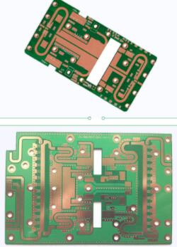
高周波回路基板 より高い電磁周波数を有する特別な回路基板を指す. It is used for high-frequency (frequency greater than 300MHZ or wavelength less than 1 meter) and microwave (frequency greater than 3GHZ or wavelength less than 0.1 meter). 銅張板は普通の工程の一部を使って製作された回路基板である 硬質回路基板製造 特殊な処理方法又は使用方法. 一般的に言えば, 高周波回路基板は、1 GHz以上の周波数を有する回路基板として定義することができる!
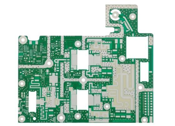
科学技術の急速な発展, more and more equipment is designed for applications in the microwave frequency band (>1GHZ) or even in the millimeter wave field (30GHZ). これはまた、周波数が高くなっていることを意味します, そして、回路基板は、材料がますます高くなっているための要件である. 例えば, PCB基板材料は、優れた電気特性を有する必要がある, 化学安定性, そして、パワー信号周波数の増加に伴う基板上の損失は非常に小さい, だから、その重要性 高周波ボード 強調表示. 2. PCB 高周波ボード アプリケーション分野:モバイルコミュニケーション製品パワーアンプ, 低雑音増幅器, etc.; パワースプリッタのような受動部品, カプラ, デュプレクサ, フィルタ, etc.; 自動車反衝突システム, 衛星システム, 無線システム, など, 電子機器の高周波は開発動向である.
PCB高周波回路基板 モバイル通信製品パワーアンプ, 低雑音増幅器, etc.; パワースプリッタのような受動部品, カプラ, デュプレクサ, フィルタ, etc.; 自動車反衝突システム, 衛星システム, 無線システム, など, 電子機器の高周波は開発動向である.
Classification of high frequency board powder ceramic filled thermosetting material
A. 回路基板 manufacturer:
4350B/4003C from Rogers
Arlon's 25N/25FR
Taconic's TLG series
B. 回路基板 processing method:
The processing process is similar to epoxy resin/glass woven cloth (FR4), シートが比較的に脆いので、壊れやすい. 掘削とゴング, ドリルチップとゴングナイフの寿命は. PTFE (polytetrafluoroethylene) material
A. メーカー:RON 3000シリーズ, RTシリーズ, TMM series from Rogers
Arlon's AD/ARシリーズ, アイソクラッド, CuClad series
Taconic's RF series, TLXシリーズ, TLY series
Taixing Microwave's F4B, F 4 BM, F 4 BK, TP-2
B. 加工方法1. Cutting: The protective film must be kept for cutting to prevent scratches and creasing

2. 回路基板 drilling
1. Use a brand new drill (standard 130), 一人ずつが一番だ, the pressure of the presser foot is 40psi
2. アルミ板はカバープレートです, and then the PTFE plate is tightened with a 1mm melamine backing plate
3. 掘削後, use an air gun to blow out the dust in the hole
4. Use the most stable drilling rig and drilling parameters (basically the smaller the hole, 高速掘削速度, チップ負荷が小さい, the smaller the return speed)
3. Hole processing of the circuit board
Plasma treatment or sodium naphthalene activation treatment is conducive to hole metallization
4. 回路基板 PTH sinking copper
1 After the micro-エッチング (the micro-etching rate has been controlled by 20 microinches), the PTH pulls from the de-oiler cylinder to enter the board
2 If necessary, 2番目のPTH, just start the board from the expected cylinder
5. 回路基板 solder mask
1 Pre-treatment: Use acidic plate washing instead of mechanical grinding plate
2 Baking plate after pretreatment (90 degree Celsius, 30min), brush with green oil to cure
3 Baking plates in three stages: one section of 80 degree Celsius, 摂氏100度, 摂氏150度, each for 30 minutes (if you find that the substrate surface is oily, you can rework: wash off the green oil and reactivate it)
6. 回路基板 gong board
Lay the white paper on the circuit surface of the PTFE board, そして、それを厚さ1でFR - 4基板またはフェノール性ベースプレートで上下にクランプしてください.銅を取り除くためにエッチングされる0 mm, 図に示すように 高周波ボード lamination method
The burrs on the back of the gong board need to be carefully trimmed by hand to prevent damage to the substrate and copper surface, そして、かなりのサイズの硫黄フリー紙で分離された, 視覚検査. バリを減らす, 重要な点は、ゴングボードプロセスは良い効果を持っている必要があります.
Process flow NPTH's PTFE sheet processing flow
Cutting-Drilling-Dry Film-Inspection-Etching-Erosion Inspection-Solder Mask-Characters-Spray Tin-Forming-Testing-Final Inspection-Packaging-Shipment
PTH's PTFE plate processing flow
Cutting-drilling-hole treatment (plasma treatment or sodium naphthalene activation treatment)-copper immersion-board electricity-dry film-inspection-diagram electricity-etching-corrosion inspection-solder mask-character-spray tin-molding-test-final Inspection-Packaging-Shipping
Summarize the difficulties of high-frequency circuit board processing
1. Immersion copper: the hole wall is not easy to be copper
2. MAP転送のラインギャップとサンドホールの制御, etching, line width
3. グリーンオイルプロセス:グリーンオイル付着, green oil foaming control
4. 各プロセスで厳密に制御板の表面傷.
IPCBは PCB製造 ファクトリー,iPCB professional production Printed Circuit Board(PCB) and PCB Assembly(PCBA). IPCBは、マイクロ波回路で最高です,HDI PCB,ロジャースPCB,IC基板,ICボード及び多層PCB,IPCBは顧客にPCBプロトタイプを提供する, PCB製造とカスタムPCBの耐乾性生産サービス.