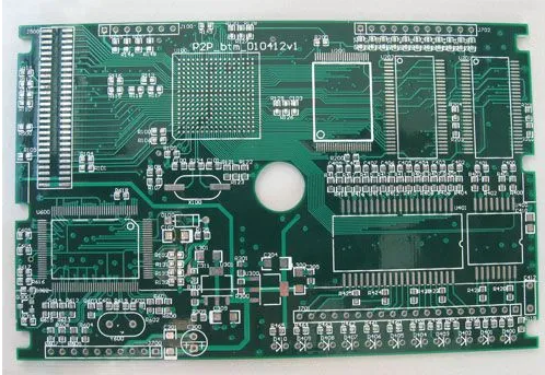
PCB回路基板 生産工程と生産 PCB製造 process
The inventor of the printed circuit board was Paul Eisler, オーストリア人, 誰が1936年に無線装置にプリント回路基板を使用したか. 1943年, アメリカ人は軍事技術で広範囲にこの技術を使った. 1948年, 米国は、商業用に本発明を公式に認めた. 1950年代半ば以降, プリント基板技術は広く採用され始めた.

プリント回路基板の出現以前, 電子部品間の相互接続は直接接続によって達成された. でも今, 回路パネルは効果的な実験ツールとして存在するプリント回路基板はエレクトロニクス産業において絶対支配的な位置を占めている.
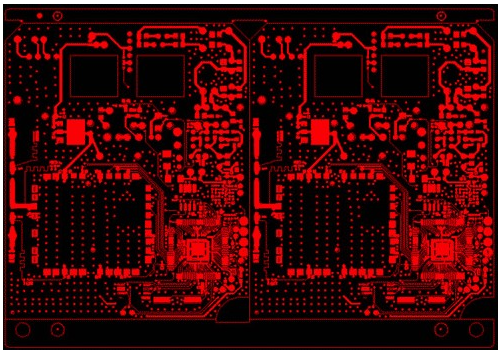
1. Detailed explanation of relevant design parameters:
one. line
1. Minimum line width: 6mil (0.153mm). 即ち, 線幅が6 mil未満であるならば, それは生産できない. デザイン条件が許可されるならば, デザインが大きい, より良い, 線幅が大きい, より良い工場, 利回りが高い, 将軍 PCB設計 ルーチンは約10ミルです. これは非常に重要です, and the design must be consider
2. Minimum line spacing: 6mil (0.153mm). 最小線距離は1行1行です, そして、線からパッドまでの距離は. 生産視点から, より大きい, 一般的なルールは10ミルです. もちろん, デザインが条件なら, より大きい. これは非常に重要です. Design Must consider
3. ラインとアウトラインラインの距離は0です.508mm (20mil)
two. via via (commonly known as conductive hole)
1. 最小開口:0.3mm (12mil)
2. The minimum via hole (VIA) aperture is not less than 0.3mm (12mil), and the single side of the pad cannot be less than 6mil (0.153mm), 好ましくは8 milより大きい (0.2mm), but not limited (see Figure 3) この点は非常に重要です, The design must be considered
3. The via hole (VIA) hole-to-hole spacing (hole side to hole side) cannot be less than: 6mil, preferably greater than 8mil. This point is very important, and the design must be considered
4. パッドとアウトラインラインの距離は0です.508mm (20mil
Third, the production process
Double-sided tin plate/immersion gold plate production process: cutting-drilling--sinking copper-circuit-drawing electricity-etching-solder mask ---Character----Spray tin (or heavy gold)-Gong edge-V cut (some boards donât need)-----Fly test----Vacuum packaging
Multi-layer tin board/immersion gold board production process: cutting-inner layer--lamination-drilling--sinking copper-circuit--map electricity- ---Etching-----Solder Mask---Character----Spray Tin (or Immersion Gold)-Gong Edge-V Cut (Some Boards Not Needed)-----Fly Test---- Vacuum packaging