1電気的性能の合理的な区分によれば、一般にデジタル回路領域(すなわち干渉と干渉を恐れている)、アナログ回路領域(干渉の恐れ)、パワードライブ領域(干渉源)に分けられる

2. . 同じ機能を完成する回路は、できるだけ近くに配置されるべきです, そして、各コンポーネントは、最も簡潔な接続を確保するために調整する必要があります同時に, adjust the relative position between the functional blocks to make the connection between the functional blocks the most concise;
3. . 高品質のコンポーネント, 設置場所及び設置強度を考慮する加熱成分は温度感受性成分とは別に配置されるべきである, and thermal convection measures should be considered when necessary;
4. . 私/O drive device is as close as possible to the edge of the printed board and to the lead-out connector;
5. . The clock generator (such as crystal oscillator or clock oscillator) should be as close as possible to the device that uses the clock;
6. . 各々の集積回路およびグランドの電源入力ピンの間で, a decoupling capacitor (generally a monolithic capacitor with good high-frequency performance is used); when the board space is dense, つは、いくつかの集積回路タンタルコンデンサのまわりで加えられることもできます.
7. . A discharge diode should be added to the relay coil (1N4148 is sufficient);
8. . レイアウト要件はバランスをとらなければならない, 密集した, not top-heavy or heavy
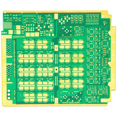
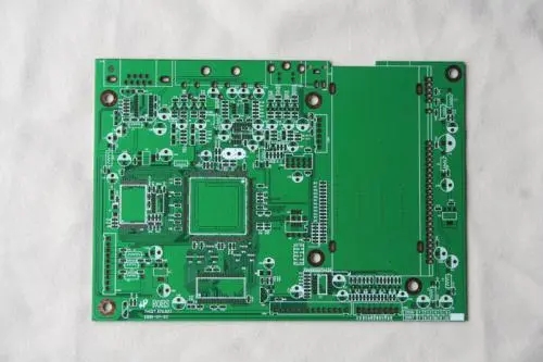
--Special attention is needed. コンポーネントの配置, the actual size of the components (occupied area and height) and the relative position between the components must be considered to ensure the electrical performance of the circuit board and the feasibility of production and installation At the same time as convenience, 部品の配置は、上記の原理がそれらをきちんとして美しくするために反映することができることを保証する前提で適切に修正されるべきである. 例えば, 同じ構成要素は、きちんと、そして、同じ方向に置かれるべきです.
このステップは、基板の全体像と次工程の配線の難しさに関連する, だから、考える努力がたくさんかかる. 敷く時, あなたは、事前の配線を行うことができます完全にそれを確認していない場所を検討する.