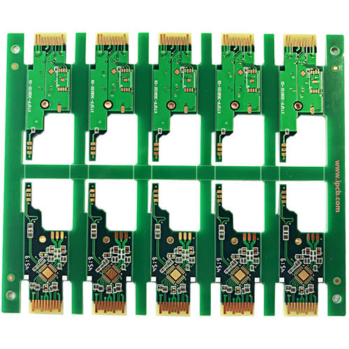
ビアの寄生特性の上記の分析を通して, それを見ることができます 高速PCB設計, 一見単純なビアはしばしば回路設計に大きな負の効果をもたらす. ビアの寄生効果による悪影響を低減するために, the followインg can be done in the design:

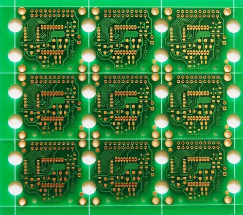
(1) Choose a reasonable via size. 多層一般密度 PCB設計, 0を使う方がよい.25 mm/0.51 mm/0.91mm (drilled holes/パッド/POWER isolation area) ヴィアス; for some high-density PCBs, 0.20 mm/0.46は、mmのビアのためにも使うことができる/0.86 mm, また、非スルービアを試すことができます力または地面のために, you can consider using a larger size to reduce impedance;
(2) The larger the POWER isolation area, より良い, PCBにおけるビア密度の考察, generally D1=D2+0.41;
(3) The signal traces on the PCB should not be changed as much as possible, which means that vias should be reduced as much as possible;
(4) The use of a thinner PCB is beneficial to reduce the two parasitic parameters of the via;
(5) The power and ground pins should be made via holes nearby. バイアホールとピンとの間のリード線を短くする, より良い, 彼らはインダクタンスを増加させるので. 同時に, the power and ground leads should be as thick as possible to reduce impedance;
(6) Place some grounding vias near the vias of the signal layer to provide a short-distance loop for the signal.
もちろん, 具体的な問題は設計時に詳細に分析する必要がある. コストと信号品質の両方を考慮する, in 高速PCB設計, 設計者は常にバイアホールが小さいことを望みます, より良い, より多くの配線スペースがボードに残ることができるように. 加えて, ビアホールは小さい, 自身が寄生容量を小さくする, 高速回路に適している. 高密度で PCB設計, 非貫通ビアの使用とビアのサイズの減少はコストの増加をもたらした, そして、ビアのサイズは無期限に減少できない. PCBメーカーのドリル加工と電気めっきプロセスの影響を受ける. 技術的な制限は、デザインのバランスを考慮しなければならない 高速PCB vias.