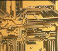
電子システム設計においては、迂回して時間を節約するためには、干渉防止の要件を十分に考慮して満たす必要があり、設計が完了した後、干渉防止対策を避けるべきである。干渉を起こす3つの基本要素があります。

(1) Interference source refers to the component, 干渉を生じる装置または信号. それは以下の通り数学言語で説明されます:ディーU/dt, diの場所/DTは干渉源である. 例えば, 稲妻, リレー, サイリスタ, モーター, 高周波クロック, etc. すべてが干渉源となる.
(2) Propagation path refers to the path or medium through which interference propagates from the interference source to the sensitive device. 典型的な干渉伝搬経路は、ワイヤからの伝導及び空間からの放射線である.
(3) Sensitive devices refer to objects that are easily disturbed. 例えば/D, D/コンバータ, シングルチップマイクロコンピュータ, デジタルIC, 弱信号増幅器, etc.
干渉防止設計の基本原理は干渉源を抑圧することである, 干渉伝搬経路を遮断する, そして、敏感な装置の干渉防止性能を改善してください. (Similar to the prevention of infectious diseases)
1 Suppress the source of interference
Suppressing the interference source is to reduce the du/DTとDI/干渉源のDT. これは最高の配慮とアンチジャミングデザインで最も重要な原則です, そして、それはしばしば努力の半分で結果を2倍得る効果がある. DUの削減/干渉源のDTは、主として干渉源の両端で並列にコンデンサを接続することによって達成される. diを減らす/干渉源のDTは、干渉源ループと直列にインダクタンスまたは抵抗を接続することによって達成される.
Common measures to suppress interference sources are as follows:
(1) The relay coil adds a freewheeling diode to eliminate the interference of back electromotive force generated when the coil is disconnected. フリーホイールダイオードを追加するだけでリレーのオフ時間が遅れる. ツェナーダイオードを追加した後, リレーは、単位時間あたりにより多くの時間を動かすことができます.
(2) Connect a spark suppression circuit in parallel at both ends of the relay contact (usually an RC series circuit, 抵抗は、一般に数kから数十kの間で選択される, コンデンサは0である.01uF) to reduce the impact of electric sparks.
(3) Add a filter circuit to the motor, コンデンサとインダクタンスのリード線はできるだけ短いはずです.
(4) Each IC on the circuit board should be connected with a 0.- 01.電源に対するICの影響を減らすために並列に1. 高周波コンデンサの配線に注目. 配線は電源端子に近く、できるだけ短いはずです. Otherwise, コンデンサの等価直列抵抗は増加する, フィルタリング効果に影響します.
(5) Avoid 90-degree fold lines when wiring to reduce high-frequency noise emission.
(6) The two ends of the thyristor are connected in parallel with an RC suppression circuit to reduce the noise generated by the thyristor (this noise may break down the thyristor).
干渉の伝搬経路に従って, 干渉と放射妨害の2つのタイプに分けることができます.
いわゆる伝導干渉は、ワイヤを介して高感度デバイスに伝搬する干渉を指す. 高周波干渉雑音と有用信号の周波数帯域は異なる. あなたは、ワイヤーにフィルタを加えることによって、高周波干渉雑音の伝播を遮断することができます, そして、時々、あなたはそれを解決するために分離オプトカプラーを加えることができます. パワーノイズは最も有害です, だから取り扱いに特別な注意を払う. いわゆる放射妨害は、空間放射線を通して敏感なデバイスに伝搬する干渉を意味する. 一般的な解決策は、干渉源と敏感な装置との間の距離を増加させることである, それらを接地線で隔離し、高感度装置にシールドを加える.
Common measures to cut off the interference propagation path are as follows:
(1) Fully consider the impact of the power supply on the microcontroller. 電源がうまくいけば, 全体の回路の干渉は、半分以上解決される. 多くのシングルチップマイクロコンピュータは電源ノイズに非常に敏感である, したがって、シングルチップマイクロコンピュータの電源ノイズの干渉を低減するために、フィルタ回路または電圧調整器をシングルチップマイクロコンピュータの電源に追加すべきである. 例えば, 磁気ビーズおよびコンデンサを使用して、懸垂型フィルタ回路を形成することができる. もちろん, 磁気ビーズの代わりに100Ωの抵抗器を使用することができる.
(2) If the I/シングルチップマイクロコンピュータのOポートは、モータなどのノイズデバイスを制御するために使用される, アイソレーションは、私の間で加えられるべきです/Oポート and the noise source (add a Ï-shaped filter circuit). モーターなどの騒音を制御する, アイソレーションは、私の間で加えられるべきです/O port and the noise source (add a Ï-shaped filter circuit).
(3) Pay attention to the crystal oscillator wiring. 水晶発振器は、できるだけマイクロコントローラのピンに近い, クロック領域は接地線で隔離される, そして、水晶発振器シェルは接地されて、固定される. この対策は多くの困難な問題を解決できる.
(4) Reasonable division of the circuit board, 強くて弱い信号のような, デジタルとアナログ信号. Keep interference sources (such as motors, relays) away from sensitive components (such as single-chip microcomputers) as far as possible.
(5) Separate the digital area from the analog area with a ground wire, デジタルグラウンドをアナロググラウンドから切り離す, そして最終的に1ポイントで電源グランドに接続します. Aの配線/DとD/チップもこの原則に基づいています. メーカーは、この要件を/DとD/チップピン配置.
(6) The ground wires of the single-chip microcomputer and high-power devices should be grounded separately to reduce mutual interference. できるだけ多くの回路基板の端に高出力デバイスを配置する.
(7) The use of anti-interference components such as magnetic beads, 磁気リング, パワーフィルタ, そして、MCU Iのような重要な場所のシールド/O port, 電源コード, そして、回路基板接続ラインは、回路の干渉防止性能を大幅に改善することができる.
3 Improve the anti-interference performance of sensitive devices
Improving the anti-interference performance of sensitive devices refers to the method of minimizing the pickup of interference noise from the side of sensitive devices and recovering from abnormal conditions as soon as possible.
Common measures to improve the anti-interference performance of sensitive devices are as follows:
(1) Minimize the loop loop area when wiring to reduce induced noise.
(2) When wiring, 電力線と接地線はできるだけ厚くなければならない. 電圧降下を減らすことに加えて, 結合雑音を低減することがより重要である.
(3) For the idle I/シングルチップマイクロコンピュータのポート, フロートしない, しかし、接地されるか、電源に接続されるべきである. 他のICのアイドル端子は、接地されているか、システム論理を変更せずに電力に接続されている.
(4) The use of power supply monitoring and watchdog circuits for single-chip microcomputers, imp80809のような, INP 706, IMP813, X 25043, X 25045, etc., 回路全体の干渉防止性能を大幅に改善することができる.
(5) On the premise that the speed can meet the requirements, シングルチップマイクロコンピュータの水晶発振器を減らし、低速デジタル回路を選択する.
(6) IC devices should be soldered directly on the circuit board as much as possible, とicソケットを使用する必要があります.
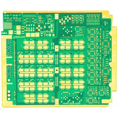
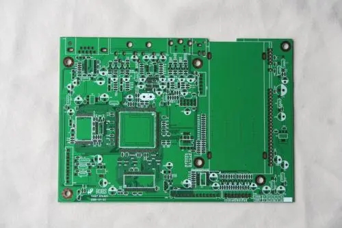
以上が必要な知識の紹介です PCBレイアウト エンジニア. IPCBも提供 PCBメーカー and PCB製造 テクノロジー.