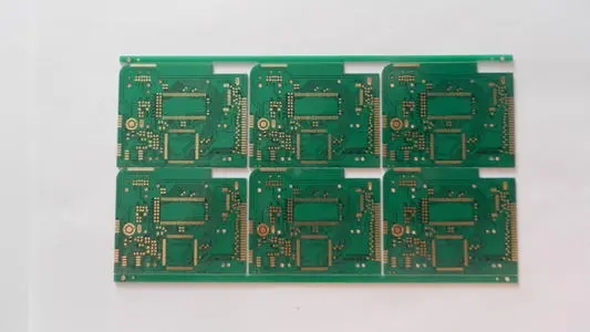
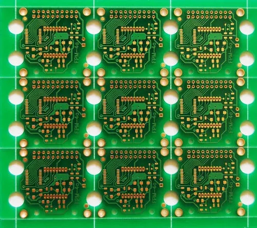
指導理念と基本配線要件 PCBレイアウト

時 PCBレイアウト, これらの材料を紹介することができます PCBレイアウト とPCBを描画するときにいくつかの共通のルール, 高品質のPCBを描く. もちろん, 実際のニーズに合わせて自由に適応できます. これは完全です PCBレイアウト デザインルール. コンポーネントのレイアウト, コンポーネントの配置, 電線の配線, 線幅と間隔, パッドだけでなく, 詳細に分析された. The following are the details:
1. Layout of components
The layout of the components of the PCB設計 規則は以下を含みます:コンポーネントレイアウト要件, コンポーネントレイアウト原理, コンポーネントレイアウト順序, and layout methods of common components
2. Arrangement of components
The arrangement of the components on the PCB can be one of three arrangements: irレギュラー, regular, グリッド, または同時に複数.
3. Spacing and installation dimensions of components
It is about the spacing between the elements and the size of the installation in the PCB設計, when the components are arranged
Four, printed wire wiring
Wiring refers to the placement of the direction and shape of the printed wires. それは、最も重要なステップです PCB設計, そして、それは最大のワークロードのステップです.
5. Width and spacing of printed wires
The width and spacing of the printed wires, 一般線の最小幅は0である.5 - 0.8 mm, and the spacing is not less than 1mm
Six, the aperture and shape of the pad
Introduce the basic knowledge of PCB設計, including the shape of the pad and the solder-like aperture
âºディーetailed parameters and basic rules
1. CLK (including DDR-CLK) basic wiring requirements:
1. CLK部分は他の線を越えることができない, そして、2つ以上のビアがありません.
2. 切ってはならない, そして、部品の2つのパッドの間で糸を通らない.
3. クリスタルの前で線を横切るな, そして、背中の上で線を横切らないようにしてください..
4. 差動ペアは、最小間隔. And on the 同じ層
5 The distance between clk and high-speed signal lines (1394, USB, etc.) should be greater than 50mil.
2. VジーA: Basic wiring requirements:
1. 赤, グリーン, そして、青は一緒に傷つけられなければなりません, 状況次第, GNDを含む. R.G.Bは横切ってはならない.
2 hsyncとvsyncを一緒に巻き込まなければならない, 適切にGNDを含む.
3. LAN: basic wiring requirements
1. 同じセットのワイヤーを一緒に巻き付けなければならない.
2ネット:RX, TX: Differential pair must be wired
4.1394: Basic wiring requirements:
1. 差動対巻線, 同じ層, 並列, 切ってはならない.
2. 同じセットのワイヤーを一緒に巻き付けなければならない.
3 The distance between the high-speed signal line and the high-speed signal line is not less than 50mil
5. USB: Basic wiring requirements:
1 Differential pair winding, same layer, 並列, 切ってはならない.
2 The same group of wires must be wound together
6. CPU-NB (AGTL): Basic wiring requirements:
1. 同じグループの同じ層または同じグループの異なる層上のワイヤ, and the wires must be wound together in the same group
2. 時巻線, the same NET spacing is not less than four times the wire width
3. NET length should be added to the package length of CPU & NB.
4. 筑波大/P(+/-) Differential Pair winding
5 VIA type is VIA26
7. CPU-SB: Basic wiring requirements:
1. 同じセットのワイヤーを一緒に巻き付けなければならない.
2プルアップ抵抗, must be close to the CPU
8. NB-DDR: Basic wiring requirements:
1. Damping resistance and terminal resistance (exclusion) NET: MD & MA & DQS & DQM cannot be shared.
2.同じグループと同じ層の配線は、間隔の4倍で巻かれる.
9. NB-AGP: Basic wiring requirements:
1. 同じグループの同じ層または同じグループの異なる層上のワイヤ, and the windings must be wound together in the same group
2. 時巻線, the same NET spacing is not less than four times the wire width
3.STB ++/差動対巻線.
4制約領域でガイドLauoutに続くようにしてください.
10. NB-SB: Basic wiring requirements:
1 一緒に歩く, 切断線を越えるな.
2. 時巻線, the same NET spacing is not less than four times the wire width
11. IDE: Basic wiring requirements:
1.同じグループと同じ層, 巻きは同じグループに一緒に巻かなければならない.
2. 時巻線, the same NET spacing is not less than four times the wire width
12. PCI: Basic wiring requirements:
1 There are at most three lines between PAD and PAD
2 Resistors and capacitors should be placed as neatly as possible.
13. CNR: Basic wiring requirements:
1.Walk together.
14. POWER: Basic wiring requirements:
1 Generally use 30: 5 wiring, 線幅は40ミル以上, 時間間隔は10 mil以下である, ビアはVIA 40です, (or 2 VIA24)
15. OTHER: Basic wiring requirements:
1. すべてのIO線は.
2. COM 1, COM 2, PRINT(LPT), 同じグループで一緒に歩く.
3 COM 1とCOM 2はコンデンサを最初に通過する, それから、ワイヤーを引いてください.
16.Add test points:
1. テストは100 %を目指していて、少なくとも98 %に加えられなければなりません.
2. ピン対ピン間隔は、好ましくは75ミルであり、最小値は50ミル.
3. テストポイントの最小パッドは27ミルです, 35ミルを使用してみてください.
4. 単層試験点と同じ層上の部分の外枠との間の距離は50 milより大きい.
5. CPUソケットはゼロレバーを含む, and no Top Side Test Point can be placed inside
6. CLKフロントエンドはテストポイントを追加する必要はありません. バックエンドはTestCount. (Require customer approval)
7. 差動対の巻線には影響しない.
17. Modify DRC:
1.DRCチェック完了, インナーチェック, そして、接続されていないピンのチェック.
2すべてのネットを短絡してはならない. 余分な線分はありません.
18. クラッディング銅箔.:
For parts that need to be coated with copper foil, 正味の銅箔を正す.
19. Place the text side:
1. テキストの表面は、左から右へと上部にマークされて, 方向は同じ.
2. パーツマーキング, 部分に近い, the better
3. 部品のピンを正しく配置し、極性をマークする.
4. 部品記号がマークされているかどうか.
CN, JP: pin mark (note the direction). Part polarity: â»Capacitor: + â»Crystal: G, D, sダイオード, 冗長ラインセグメントとラベルを削除.
上記のガイドイデオロギー入門 PCBレイアウト 基本配線要件. IPCBも提供されて PCBメーカー とPCB製造技術.