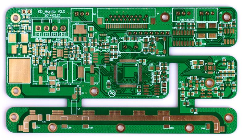
If the プリント回路基板 設計は製造可能性設計要件を満たさない, 製品の生産効率を大幅に低下させる. 深刻な場合もある, 設計された製品は全く製造できない. 現在, through-hole insertion technology (THT for short) is still in use. DFMはスルーホール挿入製造の効率と信頼性の向上に大きな役割を果たす. DFM法はスルーホール挿入メーカが欠陥を減らし,欠陥を減らすのを助ける. 競争を続ける.
1. Typesetting and layout
(1) Using a large board can save materials, しかし、反りと重さのため, 生産の輸送は難しい. それは特別な固定で修正する必要があります, so try to avoid using a board surface larger than 23cm*30cm. それは2または3の内のすべてのボードのサイズを制御することです, ガイドレールの調整によるダウンタイムを短縮するのに役立つ, バーコードリーダの位置の再配置, etc. 製品の変更時, また、基板サイズの小型化は、はんだピーク温度プロファイルの数を低減することができる.
(2) It is a good design method to include different kinds of panels in one board, しかし、1つの製品で終わり、同じ生産プロセス要件を持っているそれらのボードだけは、このように設計されることができます. Please do not copy the content of this site
(3) Some borders should be provided around the board, 特にボードの端にコンポーネントがあるとき, ほとんどの自動組立装置は、基板の縁部に少なくとも5 mmの領域を必要とする.
(4) Make wiring on the top surface (component surface) of the board as much as possible, and the bottom surface (soldering surface) of the circuit board is easily damaged. 基板の縁近くに配線しない, なぜなら、製造工程はボードの縁で掴まれるからです, そして、エッジ上の配線は、ウエーブはんだ付け装置またはフレームコンベアの顎によって損傷を受けることがある.
(5) For devices with higher pin counts (such as terminal blocks or flat cables), オーバーヘッドは、はんだ付けの間に半田ブリッジを防止するために丸い代わりに使用されるべきである.
(6) Make the spacing between the positioning holes and the distance between them and the components as large as possible, そして、挿入装置に従って彼らの寸法を標準化して、最適化してください;位置決め穴を電気メッキしない, 電気メッキ穴の直径が制御するのが難しいので.
(7) Try to use the positioning hole as the mounting hole of the PCBボード 最終製品で, 生産中の掘削工程を減らすことができる.
(8) A test circuit pattern can be arranged on the waste side of the board for process control, そして、パターンは、表面絶縁抵抗をモニタするために用いることができる, 清潔, はんだ付け性, etc. 製造工程中.
(9) For larger boards, 回路基板をウェーブはんだ付け中に中央位置に支持するために、通路を中央に残すべきである, 板をサッジングとはんだスパッタリングに防ぐ, そして、一貫して溶接される板面を手伝ってください.
(10) The testability of the needle bed should be considered in the layout design. Flat pads (without leads) can be used for better connection with the pins during online testing, すべての回路ノードがテストできるように.

2. Positioning and placement of components
(1) Arrange components in rows and columns according to a grid pattern position, すべての軸方向成分は互いに平行でなければならない, 軸挿入機が回転する必要がないように PCBボード 挿入時, 不必要な回転と運動が挿入器の速度を大いに減らすので.
(2) Similar elements shall be discharged in the same way on the board. 例えば, すべての放射状コンデンサの負極が基板の右側に面している, すべてのディップノッチマークを同じ方向に向かわせる, etc., これは挿入をスピードアップすることができますし、エラーを見つけるのは簡単になります. Aボードはこの方法を採用しているので, 逆コンデンサは容易に見つけられる, Bボード検索の時間がかかる. 実際には、すべての回路基板の向きを標準化することができます, いくつかのボードのレイアウトは、必ずしもこれを許可することはできません, しかし、それは努力でなければなりません.
(3) The arrangement direction of dual in-line package devices, コネクタ及び他の多ピン数成分は、ウエーブはんだ付け方向と垂直である, コンポーネントピン間のブリキブリッジを減らすことができる.
(4) Make full use of silk screen printing to mark the board surface, 例えば, バーコードを貼り付けるためのフレームを描画する, 板のウェーブはんだ付けの方向を示すために矢印を印刷する, and use dotted lines to trace the outline of the components on the bottom surface (so that the board only needs to be screen printed) etc.
(5) Draw the component reference character (CRD) and polarity indication, コンポーネントが挿入された後も、, チェックやトラブルシューティングの際に便利です。, また、良いメンテナンス作業.
(6) The distance between the components and the edge of the board should be at least 1.5 mm (3mm), これは、回路基板を転送し、はんだ, そして、周辺コンポーネントへの損害は、より少なくなります.
(7) When the distance of the components above the board surface needs to exceed 2mm (such as light-emitting diodes, ハイパワー抵抗器, etc.), ガスケットを下に加える. スペーサーなしで, これらの要素は、輸送中に「押しつぶされる」であり、使用中に衝撃及び衝撃を受けやすい.
(8) Avoid placing components on both sides of the PCBボード, これは、労働と時間のアセンブリを大幅に増加させる. コンポーネントが下側に置かれなければならないなら, 半田マスクテープのマスキング及び剥離を許容するために物理的に近接している必要がある.
(9) Try to distribute the components evenly on the PCBボード 反りを減らして、はんだ付けの間、均一に熱を分配するのを助けるために.
3. Machine insertion
(1) The pads for all components on the board should be standard and industry standard separation distances should be used.
(2) The selected components should be suitable for machine insertion. あなた自身の工場の装置の状態と仕様を念頭に置いておいてください, そして、前もって部品の包装形態を考える, マシンとのより良い協力. 奇形部品用, 包装はより大きな問題である.
(3) できれば, 可能な限り半径要素の軸型を使用する, 軸要素の挿入コストは比較的低いので, もし宇宙がとても貴重なら, ラジアル要素も好ましい.
(4) If there are only a small number of axial elements on the board, それらはすべて、半径型に変換されるべきです, と逆, 挿入プロセスを完全に除去できるようにする.
(5) When arranging the board surface, ピンの曲げ方向および自動挿入機の部品によって得られる範囲は、電気的間隔の観点から考慮すべきである, それと同時に, ピンの曲げ方向がブリキ橋につながることは確実である.
4. Wires and connectors
(1) Do not connect wires or cables directly to the PCB, コネクタを使う. ワイヤーを直接ボードにはんだ付けしなければならない, ワイヤの端部は板の端子にワイヤで終端する必要がある. 回路基板からのワイヤは、基板のある領域に集中されるべきである, それらが他のコンポーネントに影響を及ぼすのを避けるために一緒に入れ子にされることができるように.
(2) Use wires of different colors to prevent errors during assembly. 各社は独自のカラースキームを使用できる, すべてのプロダクトデータラインのハイビットのための青、および低ビットのための黄色のような.
(3) Connectors should have larger pads to provide better mechanical connection, そして、高いピン数コネクタのリードは、より簡単な挿入のために面取りされなければなりません.
(4) Avoid the use of dual-in-line package sockets. アセンブリ時間の拡張に加えて, この追加の機械的接続も長期信頼性を低下させる. メンテナンス理由のためにdipフィールド交換が必要なときだけ、ソケットを使用してください. ディップの品質は今では大きな進歩をして頻繁に置換を必要としません.
(5) Marks for identifying the direction should be engraved on the board to prevent errors when installing the connector. コネクタはんだ接合は機械的応力が集中する場所である, だから、いくつかのクランプツールを使用することをお勧めします, キーとスナップのような.
5. Whole system
(1) Components should be selected before designing the printed circuit board, これは、レイアウトを可能にし、この記事で説明されているDFMの原理を実装するのに役立ちます.
(2) Avoid using some parts that require machine pressure, ワイヤーピン, リベット, etc. 遅いインストール速度に加えて, これらの部品は回路基板を損傷することもある, そして、彼らはまた、維持されます.
(3) Use the following methods to minimize the types of components used on the board: replace a single resistor with a row resistor; replace two three-pin connectors with a six-pin connector; if the values of the two components are similar, しかし、公差は異なります, 両方の場所で低公差を持つものを使用しますボード上の様々なヒートシンクを確保するために同じネジを使用してください.
(4) Designed as a general purpose board that can be configured in the field. 中国で使用されたボードを輸出モデルに変えるスイッチを設置する, またはジャンパーを使用して別のモデルを変更する.
6. General requirements
(1) When conformal coating is applied to the circuit board, コーティングを必要としない部分は、エンジニアリングデザインの間、図面にマークされなければならない. ラインキャパシタンスに対するコーティングの効果は、設計上考慮すべきである.
(2) For through holes, 溶接効果を確実にするために, ピンと開口部の間のギャップは0の間でなければならない.25 mmと0.70 mm. より大きな孔径は機械挿入に有益である, 小さい毛細管サイズは良い毛細管効果に必要である, だからバランスは2つの間で打たなければならない.
(3) Components that have been pretreated according to industry standards should be selected. コンポーネントの準備は、生産プロセスの効率的な部分の一つです, and in addition to adding additional steps (with a corresponding risk of electrostatic damage and longer lead times), また、エラーの可能性を高める.
(4) Specifications should be set for most of the hand-inserted components purchased so that the lead wires on the welding surface of the circuit board do not extend beyond 1.5mm. これは、コンポーネントの準備を減らし、トリミング努力をリード, 基板はウエーブはんだ付け装置を通る.
(5) Avoid using snaps to install smaller mounts and radiators, これは遅いし、ツールが必要. If possible, 袖を使う, プラスチッククイックリベット, 両面テープ, または機械接続のためのはんだ接合を使用する.
7. Conclusion
DFM is an extremely useful tool for manufacturers who use through-hole technology for circuit board assembly, これは多くのお金とトラブルを節約できます. DFM法を用いることにより,将来のエンジニアリング変更を低減し,設計上の譲歩を行うことができる. これらの利点は、デザインの非常に直接的です PCBボード.