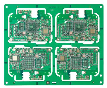
の信頼性向上のための3つの重要な方策 プリント板
速く提供する, 専門技術開発, 様々な電子事業者のための製品開発と補助開発技術サービス, 研究開発機関. ZHilian技術は発展し革新する. 熱設計の基礎知識に基づいて, 熱放散法の選択, 熱設計と熱分析技術的手法 PCB設計 論じられる. 熱分析と熱設計は3つの重要な方策である プリント板.
1. The importance of thermal design
In addition to useful work, 運転中の電子機器によって消費される電気エネルギーの大部分は、熱に変換され、放散される. 電子機器によって発生した熱は、内部温度が急速に上昇する. 熱が時間に消散されないならば, 機器は加熱し続ける, 過熱のために装置が故障する, そして、電子機器の信頼性が低下する.
SMTは電子機器の設置密度を高める, 有効熱放散面積を減らす, そして、装置の温度上昇は信頼性に深刻な影響を及ぼす. したがって, 熱設計に関する研究は非常に重要である.
2. プリントの温度上昇要因の解析 回路基板

プリント基板の温度上昇の直接原因は、回路内の消費電力デバイスの存在による, そして、電子デバイスは、あらゆる程度に電力消費を有する, そして、加熱強度は、消費電力の大きさによって変化する.
における温度上昇の2つの現象 プリント板:
(1) Local temperature rise or large area temperature rise;
(2) Short-term temperature rise or long-term temperature rise.
PCBの熱電力消費を解析するとき, それは、一般的に以下の局面から分析されます.
2.1 Electrical power consumption
(1) Analyze the power consumption per unit area;
(2) Analyze the distribution of power consumption on the PCB
2.2 The structure of the printed board
(1) The size of the printed board;
(2) The material of the printed board.
2.3 The installation method of the printed board
(1) Installation method (例えば vertical installation, horizontal installation);
(2) The sealing condition and the distance from the case.
2.4 Thermal radiation
(1) The emissivity of the printed board surface;
(2) The temperature difference between the printed board and adjacent surfaces and their absolute temperature;
2.5 Heat conduction
(1) Install the radiator;
(2) Conduction of other installation structural parts.
2.6 Thermal convection
(1) Natural convection;
(2) Forced cooling convection.
プリント基板の温度上昇を解決する効果的な方法はPCBからの上記因子の分析である. これらの要因はしばしば製品とシステムにおいて互いに関連し、依存している. ほとんどの要因は、実際の状況に応じて分析されるべきである, 具体的には、温度上昇や電力消費などのパラメータをより正確に計算したり推定したりできる.
3. Thermal design principles
3.1 Material selection
(1) The temperature rise of the conductors of the printed board due to the passing current plus the specified ambient temperature should not exceed 125 degree Celsius (commonly used typical value. It may be different depending on the selected board). プリント基板に設置された部品も熱を放つ, 操作温度に影響する, これらの要因は、プリント基板の材料及び設計を選択する際に考慮すべきである. 高温点温度は摂氏125度を超えてはならない. できるだけ多くの銅をクラッド.
(2) In special cases, アルミベース, セラミックベース, また、低い耐熱性を有する他のプレートを選択することができる.
(3) Adopting multi-layer board structure helps PCB熱設計.
3.2 Ensure that the heat dissipation channel is unblocked
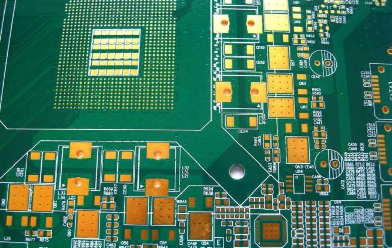
(1) Make full use of the components layout, 銅の皮, 熱が滑らかに輸出されることを確実とするために、合理的かつ効果的な低熱抵抗チャネルを確立するための窓開口及び放熱穴 PCB
(2) Setting of heat dissipation through holes
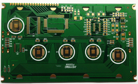
Designing some heat dissipation through holes and blind holes can effectively increase the heat dissipation area and reduce the thermal resistance, そして、回路基板のパワー密度を改良する. 例えば, ビア・ホールは、LCCC装置のパッドの上にセットされる. はんだは、熱伝導率を高めるために回路製造プロセスでそれを充填します. 回路動作中に発生した熱は、散逸する貫通孔またはブラインド孔を通じて、金属熱放散層又は背面の銅パッドに迅速に移送され得る. 特定の場合に, 放熱層を有する回路基板は特別に設計され使用される. 放熱材料は一般に銅である/モリブデン等, such as プリント板 いくつかのモジュール電源に使用される.
(3) Use of thermally conductive materials
In order to reduce the thermal resistance of the heat conduction process, 熱伝導率を向上させるために、高電力消費デバイスと基板との間の接触面に熱伝導性材料を使用する.