Статус применения технологии упаковки на уровне пластины (WLCSP) и анализ перспектив рынка в 2021 году.
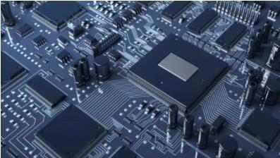
Усовершенствованная герметизация интегральных схем самой современной упаковки и технологий. В настоящее время упаковка со структурой флип-чипа (FC), упаковка на уровне пластины (WLP), 2.5D-упаковка, 3D-упаковка считаются продвинутой категорией упаковки.

Advanced packaging development circuit diagram
The overall полупроводниковое уплотнение market is expected to grow in revenue at a compound annual growth rate (CAGR) of 5.2% from 2018 to 2024, while the advanced packaging market is expected to grow at a CAGR of 8% and the market size will grow to $40 billion by 2023. The traditional packaging market, on the other hand, is growing at a cagR of less than 3.3%. Among the various advanced packaging platforms, 3D silicon through hole (TSV) and fan-out (FAN-out) packages will grow by 29% and 15%, respectively. перевёрнутый кристалл, занимать большую часть высокого упаковочного рынка, will grow at a compound annual growth rate of about 8 per cent. веер в WLP, meanwhile, will also grow at a CAGR of 8 per cent, в основном движущийся рынок.
прогноз объема глобального рынка передовой технологии упаковки, 2018-2024 (us $1 billion)

In addition, there is a growing trend to combine front-end wafer manufacturing with advanced back-end packaging. Major global wafer manufacturers (such as Intel, TSMC and Samsung) have closely combined advanced wafer manufacturing technology with advanced packaging forms to strengthen the technology integration advantages of IC product manufacturing. Influenced by both technology and scale, непрерывно повышается концентрация в глобальной отрасли герметизации и испытаний. Before 2017, eight sealing and testing enterprises (including the back-end packaging business of founds) occupied about 87% of the advanced packaging market share.
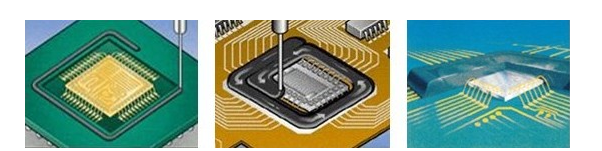
Wafer level chip size Packaging (WLCSP), как передовой метод упаковки, meets the needs and trends of consumer electronics development (light, small, short, thin and low price). Compared with traditional packaging, WLCSP packaging has the following main advantages: (1) WLCSP optimized the packaging industry chain. In the traditional packaging method, чип был сначала разрезан на зернистый чип. After being tested as a qualified chip, the wafer is placed on the lead frame or packaging substrate (substrate), and then the packaging test is carried out. промышленная цепь включает в себя вафельные фабрики, substrate factory, sealing factory and testing factory. The wafer size packaging is to encapsulate and test the wafers, and then cut the wafers after the encapsulation and test. Compared with traditional packaging, WLCSP packaging can integrate the substrate factory, packaging factory and test factory in the traditional packaging industry chain into one, so that the chip production cycle is greatly shortened, the production efficiency is improved, and the production cost is reduced. Secondly, WLCSP package can reduce the testing of qualified chips before packaging, and can effectively reduce the packaging cost; Finally, THE WLCSP package is an extension of wafer manufacturing technology, which greatly reduces the technical difference between the semiconductor back segment (packaging) and the front segment (wafer manufacturing), техническая стыковка задней части полупроводника с передней. упаковка WLCSP может быть дизайн интегральных схем, wafer manufacturing, проверка упаковки, substrate factory into one, optimize the industrial chain, solve the problem of technical and standard docking in IC design, wafer manufacturing, packaging testing, фабричное звено, and further promote the development of professional foundry mode.
количество вафли и их распределение по коммерческим моделям с использованием современных пломб (эквивалент 12 дюймов) в 2018 году

¡ The packaging cost decreases with the increase of the number of chips on the wafer. Wafer level chip size packaging is to package the entire wafer and then cut the chip, традиционный способ упаковки состоит в том, чтобы сначала разрезать вафли на чипы, затем выполните герметизацию кристалла. Generally speaking, the packaging cost of WLCSP is measured according to the number of wafers, количество чипов после резки не обязательно связано с традиционной упаковкой, стоимость упаковки определяется по количеству кристаллов в упаковке. Therefore, the packaging cost of WLCSP decreases as the wafer size increases and the number of chips increases. In the consumer electronics market development trend of light, small, short, thin, wafer level chip size packaging cost advantage is more obvious, постепенно узурпировать рыночную долю традиционной упаковки.
¢WLCSP will become the mainstream packaging method in the future. The industry believes that 3d packaging technology based on silicon through hole (TSV) is the main solution beyond Moore's Law, Это будущее развитие событий полупроводниковое уплотнение technology. WLCSP packaging is the basis of silicon through hole technology, and the two processes are very similar. By mastering WLCSP packaging technology (especially Shellcase series WLCSP), we can quickly enter the field of silicon through hole technology and play a major role in the future 3D packaging technology.
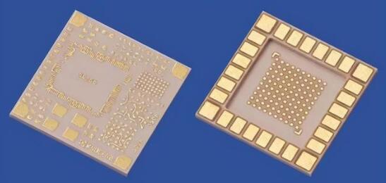
The difference between wafer level chip size package and traditional package

Yole Development forecasts that the WLCSP package market will grow from approximately $1.4 billion in 2010 to $3.2 billion in 2018 at a compound annual growth rate of 12%, около 11% усовершенствованных пакетов и около 6% глобальной отрасли закрытого тестирования. Driven by demand for small size chips such as consumer electronics and automotive electronics, we expect the WLCSP package market to reach approximately $3.5 billion in 2019, Ожидается дальнейший рост.
WLCSP mainly adopts wafer bump packaging and Shellcase series WLCSP packaging technology. пломбирование вафли на выпуклой точке является одной из форм герметизации WLCSP, и технические трудности относительно невелики. главная особенность схемы и паяльного диска может быть извлечена непосредственно из лицевой стороны чипа. серия Shellcase WLCSP не только может привести схему и диск непосредственно к лицевой стороне кристалла, можно также подключить схему чипа к обратной стороне чипа, а затем сделать сварочный диск. Shellcase series WLCSP package includes the key technical points of the wafer bump package, which is more difficult than the wafer bump package, Кроме того, этот процесс более сложен, чем пломбирование вафли. из - за технических трудностей и значительных различий в области применения, the unit price of wafer bump packaging technology is lower than Shellcase series packaging technology. Shellcase series WLCSP has excellent advantages in image sensor packaging, В то время как крышка вафли выпуклые точки не может быть использована в таких областях, как датчик изображения, из - за фасада кристалла.
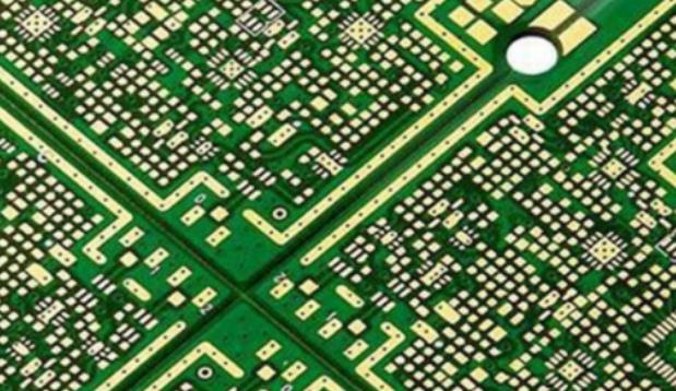
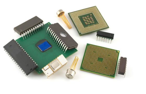
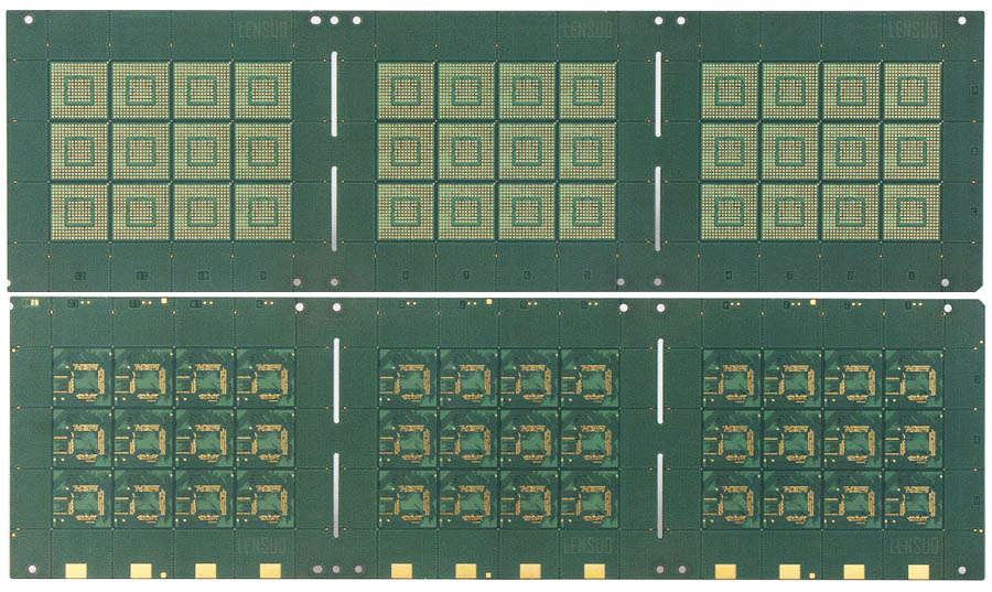
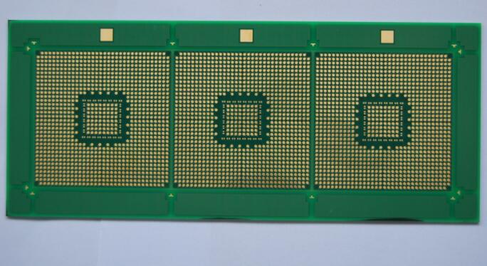
IPCB Circuit является профессиональным высокоточным производителем печатных плат R & D, серийное производство 4 - 46 слоев печатных плат, плат цепи, печатных плат, высокочастотных пластин, высокоскоростных плат, плат HDI, печатных плат, высокочастотных высокоскоростных плат, загрузки печатных плат IC. плата, полупроводниковый испытательный щиток, многослойная печатная плата, печатная плата HDI, печатная плата смешанного напряжения, высокочастотная печатная плата, мягкая и жесткая плата и т. д.
В 2018 году объем рынка упаковочных материалов составил почти 7 миллиардов долларов.