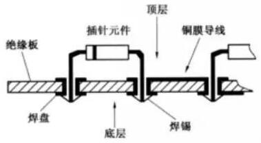
這個 印刷電路板 設計師指定的鑽孔尺寸代表製造商的最終尺寸. 由於穿透電鍍, 這個 印刷電路板 尤其是表面光潔度和銅沉積, 鑽孔直徑必須更大,以最終達到所需尺寸. 無環形環的電鍍貫穿鑽孔對最終 印刷電路板 產品.

這個 印刷電路板 用於製造的鑽孔餘量 印刷電路板(印刷電路板) may vary among manufacturers. 在 印刷電路板 外層, 0的容差.3 mm for drill pads (plus the final diameter) by default is considered as sufficient. 對於低成本 印刷電路板 大規模生產可能需要更大的餘量.
製造中的鑽孔餘量示例 印刷電路板(印刷電路板):
Surface finish chemical gold:drill allowance +0.10 mm to +0.20 mm
Surface finish chemical tin:drill allowance +0.10 mm to +0.20 mm
Surface finish HAL (non-leaded):drill allowance +0.15 mm to +0.25 mm
If an allowance of 0.應用15 mm, 環形環寬度為0.075 mm only (standard width: 0.3 mm加上 印刷電路板drill-hole).
所需尺寸:0.3 mm最終直徑/0.6 mm墊片=0.15 mm環形環
製造尺寸:0.45 mm鑽孔直徑/0.6 mm墊片=0.075 mm環形環
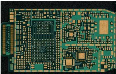
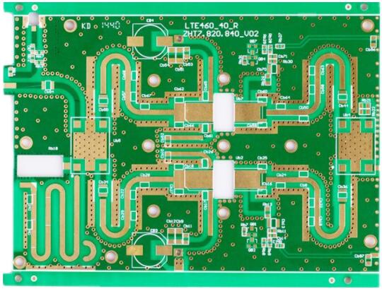
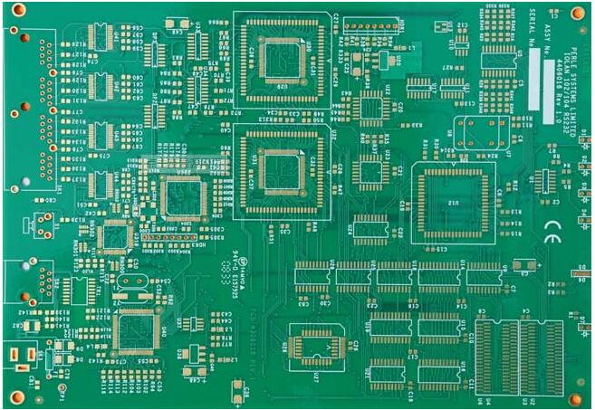
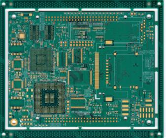
iPCB愛彼電路 電路公司., 有限公司. (iPCB愛彼電路®) is a High-Tech Manufacturing Enterprises focusing on the development and production of high precision 印刷電路板. 致力於國內外科技企業, 最複雜的 印刷電路板 製造服務業. 工廠占地23平方米,000平方米, 其中專業科技人員比例, 以及具有學士學位或. 公司在年建立了銷售網路, 香港, 韓國和其他國家, 使用科技, 以質量和服務為導向, 提供高品質 印刷電路板 處理.