什麼是 阻抗 到 印刷電路板 電路板, 為什麼 印刷電路板 需要 阻抗? 本文首先介紹 阻抗 和 阻抗 類型為, 然後介紹了原因 印刷電路板 需要 阻抗, 最後解釋了 阻抗 到 印刷電路板電路板. 跟隨編輯器瞭解更多資訊.
01
What is 阻抗
在有電阻的電路中, 電感, 和電容, 交流的障礙叫做 阻抗. 阻抗通常用Z表示, 這是一個複數. 真正的部分叫做阻力, 虛部叫做電抗. 電路中電容對交流電的阻礙作用稱為電容電抗, 電路中電感對交流電的阻礙作用稱為電感電抗, 電路中電容和電感對交流電的阻礙作用統稱為電抗. 組織為 阻抗 is歐姆.
02.
Impedance type
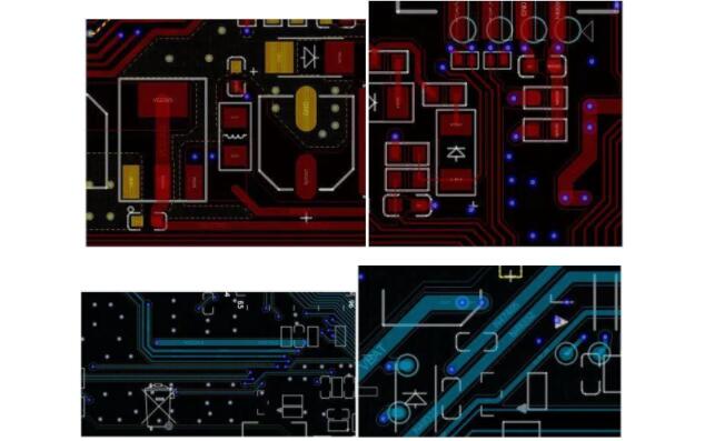
(1) Characteristic 阻抗
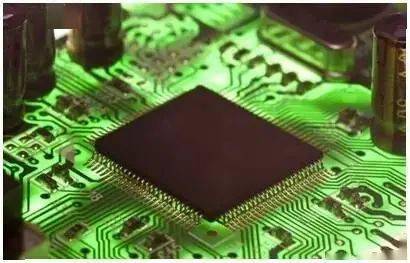
在電腦和無線通訊等電子資訊產品中, 在中傳輸的能量 印刷電路板 circuit is a square wave signal (called pulse) composed 屬於 voltage and time. 它遇到的阻力叫做特性 阻抗.
(2) Differential 阻抗
驅動端輸入兩個極性相反的相同訊號波形, 分別由兩條差分線路傳輸, 兩個差分訊號在接收端相减. 差速器 阻抗 是 阻抗 兩條導線之間的Zdiff.
(3.) Odd mode 阻抗
這個 阻抗 兩條線中一條線對地的值與 阻抗 兩行的值.
(4.) Even mode 阻抗
驅動端輸入兩個相同極性的相同訊號波形, 以及 阻抗 兩條導線連接在一起時的Zcom.
(5) Common mode 阻抗
這個 阻抗 兩條線中的一條到地面的Zoe與 阻抗 兩行的值, 通常大於奇數模式 阻抗.
03
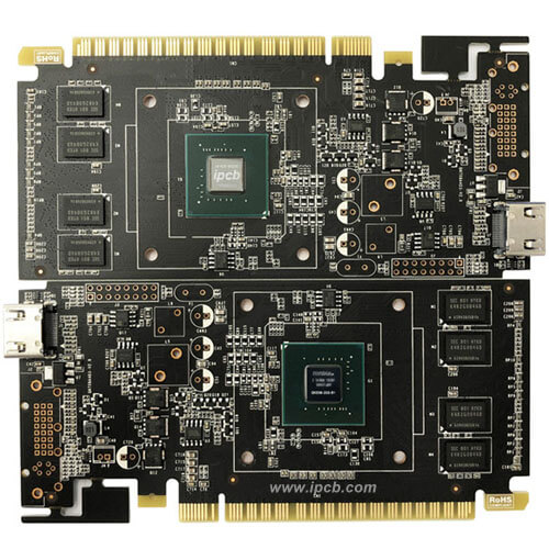
Why do 印刷電路板 電路板 need 阻抗
這個 阻抗 of 印刷電路板 電路板是指電阻和電抗的參數, 阻礙交流. 在生產過程中 印刷電路板 電路板, 阻抗 處理至關重要. 這個 reasons are as follows:
1. The 印刷電路板 circuit (bot到m of 這個 board) should consider plugging and installing electronic components. 封堵後, 應考慮電導率和訊號傳輸效能. 因此, 較低的 阻抗, 更好的, 電阻率應小於每平方釐米1. -6或更少.
2. 在生產過程中, 印刷電路板 電路板必須經過沉銅等工藝步驟, tin electroplating (or chemical plating, or thermal spray tin), 連接器焊接, 等., 這些連結中使用的資料必須確保電阻率低, 為了確保 阻抗 電路板厚度低,滿足產品品質要求,能正常工作.
3. 鍍錫 印刷電路板 電路板是整個電路板生產中最容易出現的問題, 這是影響 阻抗. The biggest defect of the electroless tin coating is easy discoloration (easy to be oxidized or deliquescent) and poor solderability, 這將導致電路板焊接困難, 高的 阻抗, 導電性差, 或董事會整體績效不穩定.
4. 中的導體中有各種訊號傳輸 印刷電路板 電路板. 當需要新增其頻率以新增其傳輸速率時, 如果電路本身因蝕刻等因素而不同, 堆疊厚度, 導線寬度, 等., the 阻抗 值將更改., 使其訊號失真,電路板效能下降, 囙此,有必要控制 阻抗 一定範圍內的值.
04
The meaning of 阻抗 to 印刷電路板電路板

For the electronics industry, 根據行業調查, the most fatal weakness of the electroless tin coating is its easy discoloration (easy to be oxidized or deliquescent), 釺焊效能差導致焊接困難, 和高 阻抗 導致電路板整體效能導電性差或不穩定., 長錫須容易導致短路 印刷電路板 甚至燒毀或起火.
據報導,20世紀90年代初,昆明理工大學在國內首次開展了化學鍍錫的研究, followed by Guangzhou Tongqian Chemical (enterprise) in the late 1990s. 到現在為止, 業界已經認識到這兩個機构是最好的. 其中, 根據我們的連絡人篩選調查, 許多公司的實驗觀察和長期耐久性測試, 經證實,通前化工的錫層為低電阻率的純錫層, 導電性和釺焊質量可保證在較高水準. 難怪他們敢於向外界保證塗層可以保持顏色一年, 無起泡, 無剝落, 和永久性錫須,無任何密封和防變色保護.
後來, 整個社會生產產業發展到一定程度, 許多後來的參與者經常相互複製. 事實上, a considerable number of companies themselves did not have the R&D or initiative capabilities themselves. 因此, many products and their usersâ electronic products (circuit boards) The bottom of the board or the overall electronic product) performance is poor, 而表現不佳的主要原因是 阻抗 問題, 因為在使用不合格的化學鍍錫工藝時, 它實際上是鍍錫在 印刷電路板 circuit board It is not really pure tin (or pure metal element), but tin compound (that is, 它根本不是金屬元素, 而是一種金屬化合物, 氧化物或鹵化物, or more directly a non-metal substance) or tin A mixture of compound and tin metal element, 但是用肉眼很難找到
因為 印刷電路板 電路板為銅箔, 銅箔的焊點上有一層鍍錫層, and the electronic components are soldered on the tin-plated layer through solder paste (or solder wire). 事實上, 焊膏正在熔化. The state soldered between the electronic component and the tin plating layer is metal tin (that is, the metal element with good conductivity), 囙此,可以簡單地指出,電子元件連接到 印刷電路板 通過鍍錫層, 所以鍍錫層的純度和 阻抗 儀器的效能是關鍵; 但在電子元件插入之前, 當我們直接使用儀器檢測 阻抗, 事實上, the two ends of the instrument probe (or called the test lead) first touch the copper foil on the bottom of the 印刷電路板 board. 然後將表面上的鍍錫層連接到 印刷電路板 傳達當前. 因此, 鍍錫是關鍵, 影響 阻抗 以及影響整個 印刷電路板, 這也是容易被忽視的關鍵.
我們都知道, 除了簡單的金屬物質, its compounds are poor electrical conductors or even non-conductive (also, this is also the key to the distribution capacity or spreading capacity in the circuit), 囙此,在錫化合物或混合物的鍍錫中,存在這種准導電性而不是導電性, 現有電阻率或電解反應後由於未來氧化或潮濕而產生的電阻率,以及相應的 阻抗 are quite high (enough to affect the level or signal transmission in the digital circuit) and The characteristic 阻抗 也不一致. 囙此,它將影響電路板和整個機器的效能.
因此, 就當前的社會生產現象而言, 底部的塗層材料和效能 印刷電路板 董事會是影響該特性的最重要和最直接的原因 阻抗 of 整個印刷電路板. 易變性, 因此 阻抗 變得更加無形和多變. 其隱匿的主要原因有:一是, it cannot be seen by the naked eye (including its changes), 其次, 由於其隱蔽性,無法持續量測. 變異性隨時間和環境濕度變化, 所以它總是很容易被忽視.