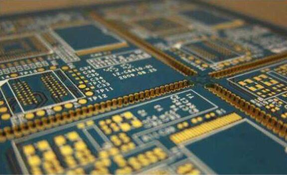
現時, 在 PCB製造 印刷電路板, 這些電線大多是銅線. 銅金屬本身的物理特性决定了在導電過程中必須有一定的阻抗. 導線中的電感元件將影響電壓訊號和電阻的傳輸. 該部件將影響電流訊號的傳輸, 高頻線路中電感的影響尤為突出.

印刷電路板上的某一條導線可以被視為非常規則的矩形銅帶. 讓我們拿一根10釐米長的金屬絲, 1.5mm寬, 以50mm厚為例. 通過計算可以看出阻抗. .
The wire resistance can be calculated by the formula:
R=ÏL/s (Ω)
where L is the length of the wire (meters), s is the cross-sectional area of the wire (square millimeters), Ï是電阻率Ï=0. 02. 計算得出導線的電阻值約為0.026Ω.
當遠離其他導體的一段導線比其寬度長得多時, 導線的自感係數為0.8m小時/m, 然後一根10cm長的導線的電感為0.08m小時. Then we can use the following formula to find the inductive reactance presented by the copy board wire:
XL=2ÏfL
where Ï is a constant, f is the frequency of the signal passing through the wire (Hz), 和 L is the self-inductance per unit length of the wire (H). 以這種管道, we can calculate the inductance of the wire at low frequency and high frequency respectively:
When f=10KHz, XL=6.28*10*103*0. 08*10-6â 0. 005Ω;
When f=30MHz, XL=6.28*30*106*0.08*10-6â 16Ω
Through the above formula calculation, 我們可以看到,在低頻訊號傳輸中,導線電阻大於導線電感, 而在高頻訊號中,導線電感遠大於導線電阻.
以上是導線阻抗干擾分析的介紹 PCB複製板設計. Ipcb也提供給 PCB製造商 and PCB製造 科技