PCB電路設計 and pre-production operations (basic knowledge)

1. Annular Ring
Refers to the copper ring that is flatly attached to the board surface around the wall of the through hole. 內板上的孔環通常通過跨橋連接到外接地, 通常用作線路或車站的終點. 在外層板上, 它可以用作元件引脚焊接的焊墊, 除用作電路交叉站外. There are Pad (with circle), Land (independent point) and so on that are synonymous with this word.
2. Artwork film
In the circuit board industry, 這個詞通常指黑白否定詞. As for the brown "Diazo Film" (Diazo Film), 它也以Phototool命名. 印刷電路板中使用的底片可分為“原始底片”原圖和重新拍攝的“工作底片”工作圖, 等.
3. Basic Grid
Refers to the vertical and horizontal grid where the conductor layout of the circuit board is designed. 早期, 網格間距為100密耳. 現時, 由於細紋和密集紋的普遍存在, 基本網格間距已减少到50密耳.
4. Blind Via Hole
Refers to the complex 多層PCB板, 因為部分過孔只需要一定的互連層, 所以他們故意鑽得不完整. 如果其中一個孔連接到外板的環上, 它就像一個杯子,死胡同中的特殊孔被稱為“盲孔”.
5. Block Diagram circuit system block diagram
The assembly board and the various components required are framed in square or rectangular empty boxes on the design drawing, 並且使用各種電符號逐個地傳達幀之間的關係,以形成系統結構圖.
6. Bomb Sight bullet mark
Originally refers to the aiming screen where bombers dropped bombs. 在製作 PCB板, 為了對齊, 在每個角上還設定了上下兩層對齊目標. 更準確的官方名稱應稱為攝影師的目標.
7. Break-away panel can be disconnected
Refers to many small-area circuit boards. 為了方便插入, 組件放置, 下游裝配線上的焊接和其他操作, 在PCB製造過程中, 它們被專業組合在一塊大電路板上進行各種處理. 工作完成時, the method of jumping blades is used to perform a local cutting shape (Routing) disconnection between the independent small plates, 但保留了幾個具有足够强度的“拉杆或分離片”, 它們是相互聯系的. 在板材和板材邊緣之間再鑽幾個小孔; 或上下切割V形槽口,以便於組裝過程完成後分離電路板. 這種小型板接頭組裝方法在未來將越來越多, IC卡就是一個例子.
8. Buried Via Hole
Refers to the local vias of the multilayer board. 當它們埋在多層板的內層之間時, 它們成為“內部通孔”,不與外部板“連接”, 它們被稱為埋入式過孔或埋入式過孔.
9. Bus Bar
Refers to the cathode or anode rod itself on the electroplating tank, 或其連接的電纜. 在電路板中“進行中”, 金手指的外邊緣靠近板的邊緣, the original connecting wire (which must be covered during the gold plating operation), and a small narrow piece (all for saving gold (It is necessary to minimize the area) to connect with each finger. 這種導電連接也稱為母線. 每個手指連接到母線的小片稱為射棒. 當板材完成形狀切割時, 兩者將同時被切斷.
10. CAD computer-aided design
Computer Aided Design uses special software and hardware to digitally lay out the circuit board, 並使用光學繪圖器將數位資料轉換為原始膠片. 這種CAD對於電路板的預製造工程來說,比手工方法要精確和方便得多.
11. Center-to-Center Spacing
Refers to the Nominal Distance (Nominal Distance) from the center to the center of any two conductors on the board. If the conductors arranged in a row have the same width and spacing (such as the arrangement of gold fingers), 那麼這個“中心到中心的間距”也被稱為節距.
12. 淨空室, 清除, empty ring
Refers to the inner layer of the multilayer board, 如果導體表面未與通孔的孔壁連接, 通孔周圍的銅箔可以蝕刻掉,形成一個空環, 特別是所謂的“空環”. 此外, 印製在外板上的綠色油漆與每個環之間的距離也稱為間隙. 然而, 由於電流板表面密度逐漸新增, 這種綠色油漆的原始房間也被迫幾乎空無一人.
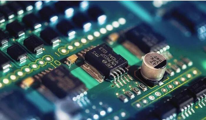
13. Component Hole
Refers to the through-holes for inserting parts on the board. 該銷孔的孔徑平均約為40密耳. 現在SMT已經很流行了, 大孔徑千斤頂的數量已逐漸减少, 連接器上只有幾個金針孔需要塞焊, 剩下的大部分SMD部件都是表面貼裝的.