佈局/裝電線, 對電力效能的影響經常出現在有關電子的書籍中, 說“數位地線和類比地線應該分開”. 部署董事會的每個人都知道,這在實際操作中是有一定難度的.
佈置更好的董事會, 您必須首先對正在使用的集成電路有電力方面的瞭解, which pins will produce higher harmonics (the rising/falling edges of digital signals or switching square wave signals). 哪些引脚容易受到電磁干擾, the signal block diagram (signal processing unit block diagram) inside the IC helps us understand.

整機佈局是確定電力效能的主要條件, 電路板的佈局更關注訊號的方向或流量/ICs之間的數據. 主要原理是靠近電源的部分容易受到電磁輻射; 有許多弱信號處理部分. Determined by the overall structure of the equipment (that is, the overall planning of the equipment in the early stage), as close as possible to the input end of the signal or the detection head (probe), 它可以更好地提高信噪比,為後續的信號處理和數據識別訊號提供更純淨的訊號/正確無誤的資料.
2. PCB銅線 鉑加工. As the current IC working clock (digital IC) is getting higher and higher, 其訊號對線路寬度提出了一定要求. The width of the trace (copper platinum) is good for low frequency and strong current. 但對於高頻訊號和數據線訊號, 事實並非如此. 數據訊號更多的是關於同步, 高頻訊號主要受趨膚效應的影響. 因此, 兩者必須分開.
高頻訊號軌跡應薄而不是寬, 短而不是長, which also involves layout issues (signal coupling between devices), 可以减少感應電磁干擾.
數據訊號以脈衝形式出現在電路上, and its high-order harmonic content is the decisive factor to ensure the correctness of the signal; the same wide copper platinum will produce a skin effect (distribution) for the high-speed data signal. 電容/inductance becomes larger), 這將導致訊號惡化, 數據識別不正確, 如果數据總線通道的線寬不一致, it will affect the synchronization problem of the data (causing inconsistent delay), 為了更好地控制數據訊號, 數据總線路由中出現一條蛇形線, 這是為了使數據通道中的訊號在延遲上更加一致.
大面積鋪銅用於遮罩干擾和感應干擾. 雙面板可以讓地面用作鋪銅層; 而多層板不存在鋪銅的問題, 因為中間的功率層非常好. 遮罩和隔離.
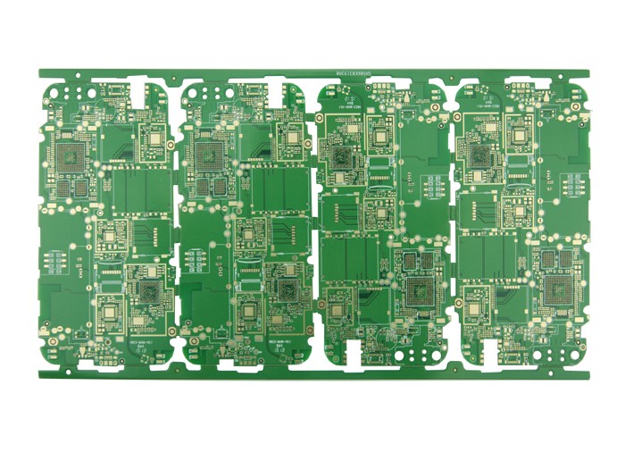
3. Interlayer layout of multilayer board
Take a four-layer board as an example. The power (positive/negative) layer should be placed in the middle, 訊號層應在外部兩層佈線. 注意,正負功率層之間不應有訊號層. 這種方法的優點是盡可能, 讓功率層發揮濾波作用/遮罩/隔離, 同時方便PCB生產廠家提高良品率.
4. Via
Engineering design should minimize the design of vias, 因為過孔會產生電容, 還有毛刺和電磁輻射. The aperture of the via hole should be small but not large (this is for electrical performance; but too small aperture will increase the difficulty of PCB生產, 一般為0.5毫米/0.8mm, 0.3mm is used as small as possible), 小孔徑用於浸銅過程,後續毛刺的概率小於大孔徑. 這是由於鑽井過程.
5. Software application
Every software has its ease of use, 這只是你對軟件的熟悉程度. I have used PADS (POWER PCB)/PROTEL公司. When making simple circuits (the circuits I am familiar with), 我會使用PADS直接佈局; 在製作複雜的新設備電路時, 最好先畫示意圖, 並以網絡清單的形式進行, 這應該是正確和方便的.
佈局PCB時, 有一些非圓孔, 軟件中沒有相應的功能可描述. 我通常的方法是:打開一層專業用來表達的洞, 然後在此層上繪製所需的開口. 孔形狀, 當然, 應填充拉絲框架. 這是為了更好地讓PCB製造商識別自己的表達,並在示例檔案中進行解釋.
6. The PCB is sent to the manufacturer for sample
1. PCB computer files
2. The layering scheme of the PCB file (each electronic engineer has different drawing habits, 佈局後的PCB檔案在層應用中會有所不同, 所以你需要附上一張白油圖/綠油圖/檔案的電路圖 /機械結構圖/輔助孔圖紙, make a correct list document to explain your wishes)
3. PCB生產 工藝要求, 你需要附上一份檔案來解釋製作電路板的過程:鍍金/鍍銅/鍍錫/清掃松香, 板厚規格, PCB板材料 (flame retardant/non-flame retardant).
4. The number of samples
5. 當然, 你必須在聯系資訊和負責人上簽字