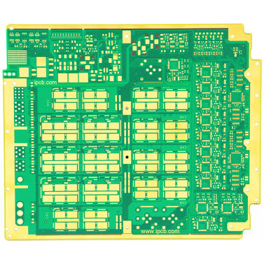
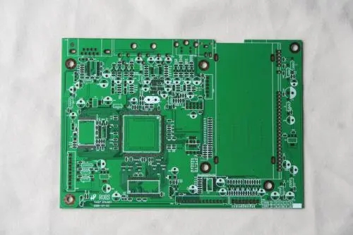
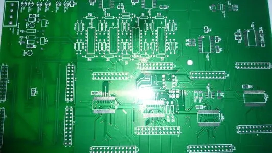
1. 根據電力效能的合理劃分,一般分為:數位電路區(即害怕干擾和干擾)、類比電路區(害怕干擾)、功率驅動區(幹擾源);

2. . 完成相同功能的電路應盡可能靠近, 應調整每個組件,以確保最簡潔的連接; 同時, adjust the relative position between the functional blocks to make the connection between the functional blocks the most concise;
3. . 用於高品質部件, 應考慮安裝位置和安裝强度; 加熱部件應與溫度敏感部件分開放置, 和 thermal convection measures should be considered when necessary;
4. . I/O drive device is as close as possible to the edge of the printed board and to the lead-out connector;
5. . The clock generator (such as crystal oscillator or clock oscillator) should be as close as possible to the device that uses the clock;
6. . 每個集成電路的電源輸入引脚與接地之間, a decoupling capacitor (generally a monolithic capacitor with good high-frequency performance is used); when the board space is dense, 還可以在幾個集成電路鉭電容器周圍添加一個.
7. . A discharge diode should be added to the relay coil (1N4148 is sufficient);
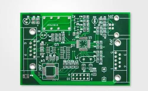
8. . 佈局要求應平衡, 密集有序, not top-heavy or heavy
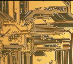
--Special attention is needed. 放置組件時, the actual size of the components (occupied area and height) and the relative position between the components must be considered to ensure the electrical performance of the circuit board and the feasibility of production and installation At the same time as convenience, 應在確保上述原則能够得到體現的前提下,對組件的放置進行適當修改,使其整潔美觀. 例如, 相同的部件應整齊地放置在同一方向上.
這一步與電路板的整體影像和下一步佈線的難度有關, 囙此,需要花費大量精力來考慮. 佈局時, 您可以進行初步佈線,並充分考慮不確定的地方.