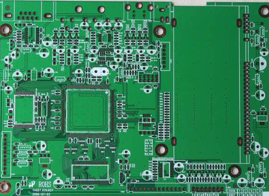
這個 outer frame (clamping side) of the PCB jigsaw should adopt a closed-loop design to ensure that the PCB jigsaw will not be deformed after being fixed on the fixture
2. The center distance between the small plates is controlled between 75 mm 和 14.5 mm

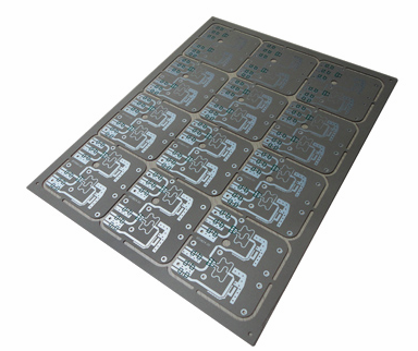
3. The PCB板 形狀應盡可能接近正方形, 和2*2*2, 3*3,, and
4. 在拼板框架的四個角上打四個定位孔, 直徑為4mm±0.01毫米; 孔的强度應適中,以確保其在上下板期間不會破裂; 孔徑和位置的精度應較高, and the hole wall should be smooth and without thorns
5. 在拼圖外框和內部小板之間的連接點附近不應有大型裝置或突出裝置, 還有小板和小板, 應該超過0.5mm space between the components and the edge of the PCB to ensure The cutting tool is operating normally
6. PCB拼板中的每個小板必須至少有3個定位孔, 3–6毫米孔徑, and no wiring or patching is allowed within 1mm of the edge positioning hole
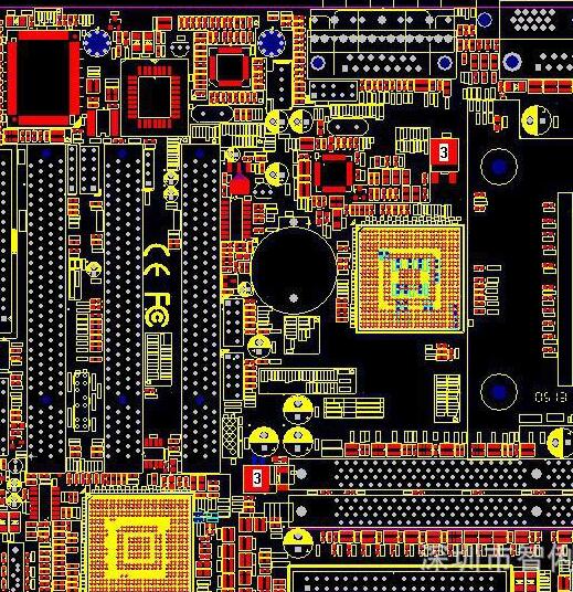
8. 用於整個PCB定位和精細間距設備定位的參攷符號. 原則上, 間距小於0的QFP.其對角線位置應設定65mm; 用於拼版PCB子板的定位參攷符號應成對使用, 佈置在定位特徵的對角.
9. 設定參攷定位點時, 通常留下非焊接掩模區域1.5 mm larger than it around the anchor point
10. PCB panel width â ¤260mm (S我EMENS line) or â ¤300mm (FUJI line); if automatic dispensing is required, PCB panel width*length â ¤125 mm*180 mm
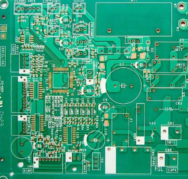
11 large components should have positioning posts or positioning holes, 比如我/O介面, 麥克風, 電池介面, 微動開關, 耳機介面, 發動機, 等.
12. I/O埠, 耳機插孔和側鍵不應盡可能多地拼接, 拼接位置應儘量選擇在直線上或圓弧較大的位置, which is conducive to processing
13. The positioning hole of the clamping edge should be more than 4-5mm from the edge of the board
14.通常,整個PCB是矩形的. 考慮PCB組件的承重, 新增了短邊和板邊.
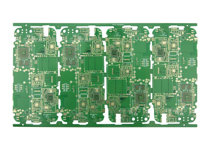
15. 根據實際工作的便利性評估拼圖塊的數量.
16.通常需要注意面板之間是否存在連接器和其他干擾.
17.通常使用AI和SMD板, 板側面預留5m~6m, and two 4*6mm positioning holes are placed on each side.
以上介紹了在使用中需要注意的要點 PCB組件. Ipcb也提供給 PCB製造商 和PCB製造技術.