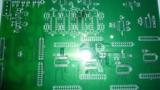
1 如何選擇 PCB板?
選擇 PCB板 must strike a balance between meeting design requirements and mass production and cost
Design requirements include electrical and mechanical parts
Usually this 材料 problem is more important when designing very 高速PCB板(frequency greater than GHz)
例如, 常用FR-4資料, the dielectric loss (dielectric loss) at a frequency of several GHz will have a great influence on the signal attenuation, 可能不合適.

就電力而言, 注意介電常數和介電損耗是否適合設計頻率
2、如何避免高頻干擾?
避免高頻干擾的基本思想是儘量減少高頻訊號電磁場的干擾, which is the so-called crosstalk (Crosstalk)
Can increase the distance between the high-speed signal and the analog signal, 或添加地面防護/shunt traces next to the analog signal
Also pay attention to the noise interference from the digital ground to the analog ground
3、如何解决高速設計中的信號完整性問題?
Signal integrity is basically a problem of impedance matching
The factors that affect impedance matching include the structure and output impedance of the signal source, 軌跡的特徵阻抗, 負載的特性, 軌跡的拓撲結構, 等.
解決方案是依靠接線的端接和調整拓撲
4、差分接線方法是如何實現的?
在差分對的佈局中需要注意兩點. 一是兩根導線的長度應盡可能長, and the other is that the distance between the two wires (this distance is determined by the differential impedance) must be kept constant, 那就是, 保持平行.
有兩種平行的管道, one is that the two wires run on the same wiring layer (side-by-side), and the other is that the two wires run on two adjacent layers above and below (over-under).
通常地, the former has more side-by-side implementations
5. 如何為只有一個輸出端子的時鐘訊號線實現差分接線?
使用差分接線, 信號源和接收器也是差分訊號是有道理的.
因此, 對於只有一個輸出端子的時鐘訊號,不可能使用差分接線.
6、能否在接收端的差分線對之間添加匹配電阻器?
通常在接收端的差分線對之間添加匹配電阻, and its value should be equal to the value of the differential impedance
This way the signal quality will be better
7、為什麼差分對的接線應緊密且平行?
The wiring method of the differential pair should be appropriately close and parallel
The so-called appropriate proximity is because this spacing will affect the value of differential impedance, which is an important parameter for designing differential pairs
The need for parallelism is also because of the consistency of the differential impedance
If the two lines are suddenly far and near, 差動阻抗將不一致, which will affect signal integrity and timing delay
8. How to deal with some theoretical conflicts in actual wiring
1. 大體上, 對類比信號進行分割和隔離是正確的/digital ground
It should be noted that the signal trace should not cross the divided place (moat) as much as possible, 電源和訊號的回流路徑不應過大.
2. 晶體振盪器是一種類比正回饋振盪電路. 要有穩定的振盪訊號, 它必須滿足環路增益和相位規格. 該類比信號的振盪規格很容易受到干擾. 即使添加了地面防護痕迹, 它可能無法完全隔離干擾.
太遠了, 接地層上的雜訊也會影響正回饋振盪電路.
因此, the distance between the crystal oscillator and the chip must be as close as possible
3. It is true that there are many conflicts between high-speed wiring and EMI requirements
But the basic principle is that the resistance and capacitance or ferrite bead added by EMI cannot cause some electrical characteristics of the signal to fail to meet the specifications.
因此, 最好使用排列痕迹和 PCB堆疊 解决或减少電磁干擾問題, such as high-speed signals through the inner layer
Finally, 電阻電容器或鐵氧體磁珠方法用於减少對訊號的損壞
9、如何解决高速訊號手動接線與自動接線的衝突?
現時, 大多數强佈線軟件的自動路由器都設定了約束條件來控制纏繞方法和過孔數量.
The winding engine capabilities and constraint setting items of various EDA companies are sometimes far from each other.
例如, whether there are enough constraints to control the way of serpentine winding, 是否可以控制差分對的軌跡間距, 等.
This will affect whether the routing method of the automatic routing can meet the designer's idea
此外, the difficulty of manually adjusting the wiring is also absolutely related to the ability of the winding engine.
For example, 軌跡的推進能力, 通孔的推動能力, 甚至微量元素對銅塗層的推動能力, etc.
因此, 選擇具有强大繞線引擎能力的路由器是解決方案.
10. About test coupon
The test coupon is used to measure whether the characteristic impedance of the produced PCB板 meets the design requirements with TDR (Time Domain Reflectometer)
通常地, the impedance to be controlled has two cases: a single line and a differential pair
因此, the line width and line spacing on the test coupon (when there is a differential pair) should be the same as the line to be controlled
The most important thing is the location of the grounding point during measurement
In order to reduce the inductance of the ground lead, TDR探頭的接地位置通常非常靠近探頭尖端. Therefore, 試樣上訊號量測點和接地點之間的距離和方法,以匹配所用探頭
11、在高速PCB設計中,訊號層的空白區域可以塗銅,多個訊號層的銅塗層應該如何分佈在地面和電源上?
通常地, most of the copper plating in the blank area is grounded
Just pay attention to the distance between the copper and the signal line when applying copper next to the high-speed signal line, because the applied copper will reduce the characteristic impedance of the trace a little
Also be careful not to affect the characteristic impedance of other layers, 例如 in the structure of the dual stripline
12. 可以使用微帶線模型計算功率平面上訊號線的特性阻抗嗎?
能否使用帶狀線模型計算電源和接地層之間的訊號?
對, 計算特性阻抗時, both the power plane and the ground plane must be regarded as the reference plane
For example, 四層板:頂層電源層底層. 此時, 頂層的特性阻抗模型是以功率面為基準面的微帶線模型
13、在正常情况下,高密度印製板上的測試點能否由軟件自動生成,以滿足批量生產的測試要求?
Generally, whether the test points automatically generated by the software meet the test requirements depends on whether the specifications for adding test points meet the requirements of the test equipment
In addition, 如果佈線過於密集,並且添加測試點的規範非常嚴格, there may be no way to automatically add test points to each segment of the line. 當然, 您需要手動填寫要測試的位置.
14. 添加測試點會影響高速訊號的質量嗎?
它是否會影響訊號質量取決於添加測試點的方法以及訊號的速度.
大體上, additional test points (do not use the existing perforation (via or DIP pin) as test points) may be added to the line or pulled out a short line from the line
The former is equivalent to adding a small capacitor on the line, the latter is an extra branch
Both of these conditions will affect the high-speed signal more or less, 影響的程度與訊號的頻率速度和訊號的邊緣速率有關.
The magnitude of the impact can be known through simulation
In principle, 測試點越小, 更好 (of course, it must meet the requirements of the test tool) the shorter the branch, the better
15、幾塊PCB組成一個系統,板之間的地線應該如何連接?
當訊號或電源在每個 PCB板 is connected to each other, for example, 如果板A有電源或向板B發送訊號, there must be an equal amount of current flowing from the ground back to board A (this is Kirchoff current law)
The current on this ground will find the place with the least impedance to flow back
Therefore, 在每個介面處, 無論是電源互連還是訊號互連, 分配給接地層的管脚數量不應太小,以降低阻抗, 可以减少地面層的譟音.
In addition, 您還可以分析整個電流回路, 尤其是電流大的部分, and adjust the connection of the ground layer or ground wire to control the current flow (for example, make a low impedance somewhere so that most of the current flows from this Place to walk) to reduce the impact on other more sensitive signals