為了確保質量 印刷電路板 設計, 在設計 PCB板, 需要注意的是 PCB板 圖符合要求.
1 Component layout
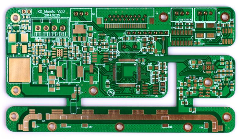
Reasonable arrangement of components is 這個 basic premise of designing a high-quality PCB layout. 部件佈置要求主要包括安裝, 武力, 熱, 訊號, 和美學.
1.1. Installation
Refers to a series of basic requirements for the smooth installation of the PCB板 進入主機殼, 套管, 和特定應用中的插槽, 避免空間干擾、短路等事故, 並將指定的連接器保持在主機殼或外殼上的指定位置. 要求. 我在這裡不談細節.

1.2. Force
The circuit board should be able to withstand various external forces and vibrations during installation and work. 因此, the PCB板 應該有一個合理的形狀, and the positions of various holes (screw holes, special-shaped holes) on the board should be reasonably arranged. 通常地, 孔和板邊緣之間的距離應至少大於孔的直徑. 同時, 還應注意,由异形孔引起的板的薄弱部分也應具有足够的彎曲強度. 特別地, 直接從板上的設備外殼“延伸”出來的連接器應合理固定,以確保長期可靠性.
1.3. Heat
For high-power devices with serious heat generation, 除了確保散熱條件外, 還應注意將其放置在適當的位置. 尤其是在複雜的類比系統中, 應特別注意這些設備產生的溫度場對脆弱前置放大器電路的不利影響. 通常地, 功率非常大的部件應製成單獨的模塊, 它與信號處理電路之間應採取一定的熱隔離措施.
1.4. Signals
Signal interference is an important factor to be considered in PCB layout design. 幾個基本方面是:弱訊號電路與强訊號電路分離甚至隔離; 交流部分與直流部分分離; 高頻部分與低頻部分分離; 注意訊號線的方向; 地線的佈置; 量測. 這些已經在大量的論文中反復強調,這裡不再重複.
1.5. Beautiful
It is not only necessary to consider the neat and orderly placement of components, 還要考慮到佈線的優美和流暢. 因為一般外行有時會強調前者, 為了片面地評估電路設計的利弊, 對於產品的形象, 當效能要求不苛刻時,應優先考慮前者. 然而, 在高性能場合, 如果必須使用雙面板, 電路板也封裝在其中, 它通常是看不見的, 痕迹的美學應該得到優先考慮. 下一節將詳細討論佈線的“美學”.
2. Wiring principles
Some anti-jamming measures not commonly found in the literature are detailed below. 考慮到在實際應用中, 特別是在產品試製中, 仍在使用大量雙面面板, 以下內容主要針對雙面面板.
2.1. Wiring "Aesthetics"
When turning, 避免直角,並嘗試使用斜線或圓弧進行過渡. 接線應整齊有序, 集中佈置, 這不僅避免了不同性質訊號的相互干擾, 也便於檢查和修改. 對於數位系統, there is no need to worry about interference between signal lines (such as data lines and address lines) of the same camp, 但控制訊號,如read, 寫, 時鐘應隔離並用地線保護. 鋪設地面時 in a large area (discussed further below), try to maintain a reasonable and equal distance between the ground wire (in fact, it should be the ground "surface") and the signal wire, 在防止短路和洩漏的前提下,儘量靠近. 對於弱電系統, 接地線和電源線應盡可能靠近. 對於使用表面安裝組件的系統, 訊號線應該一直到前面.
2.2. Ground wire arrangement
There are many discussions on the importance and layout principles of the ground wire in the literature, 但在實際應用中,對地線佈置仍缺乏詳細準確的介紹 PCB板. My experience is that in order to improve the reliability of the system (rather than just making an experimental prototype), 地線怎麼強調都不為過, 尤其是在弱信號處理中. 為此目的, 我們必須不遺餘力地貫徹“大面積鋪路”的原則. When laying the ground, 它通常必須是網格狀的, 除非這些分散的地點被其他線分割. 電網接地的熱效能和高頻電導率遠優於整個接地線. 在雙面佈線中, 有時為了佈置訊號線,必須分離接地線, 這對保持足够低的接地電阻極為不利. 為此目的, 必須使用一系列“智慧”方法來確保接地電流“平滑”. 這些技巧包括:大量使用表面貼裝組件, 消除“應該”屬於地面的空間. 充分利用正面空間:在使用大量表面安裝組件的情况下, 儘量使訊號線到達頂層, 並將底層“無私”地交給底層, 這涉及到無數的小提示, 我自己寫“PCB”的一個電路板技能:交換引脚有一個技巧, 還有很多類似的咒語, 以後會一個接一個地寫. 合理佈置訊號線, 並“給予”董事會上的重要領域, especially the "hintland" (this is related to the communication of the entire board ground line) to the ground line, 只要精心設計, 這仍然可以做到. 前後協調:有時在板的一側, 接地線真的“不可能”, 然後你可以試著使兩側的接線相互協調. 相應位置有足够的空間來鋪設地線, and then pass through enough and reasonably located vias (considering that the vias have a large resistance), 訊號線將穿過這座“橋”. 强行分開, 但不情願地, 期待統一, 海峽兩岸連成一個整體,具有足够的導電性. 狗跳牆的意義:當巨大的地線找不到地方,不願意被一條訊號線切斷時, 讓這個訊號表達不滿, 使用跨接導線. 有時, 我不願意只拉一根裸線, 該訊號恰好通過電阻器或其他“長腿”裝置, 我可以合理地擴展這個設備的引脚, 使其作為跳線具有雙重功能, 既傳遞訊號,又避免使用不恰當的跳線名稱. 當然, 在大多數情况下, 我總是可以讓這樣的訊號通過正確的地方,並避免與地線交叉需要觀察和想像. 最小原則:接地電流路徑應合理, 大電流和弱訊號電流不得並排移動. 有時, 選擇合理的路徑, 還有一排接地線一支軍隊配寘不合理. 順便說一句, 有句名言:“你可以信任你的母親, 但永遠不要相信你的立場”. In the case of extremely weak signal processing (below microvolts), 即使為了保持地電位的一致性而保證了平均值, 電路上關鍵點的接地電位差仍然超過正在處理的訊號的幅度, 至少以相同的數量級. 即使靜電勢合適, 暫態電位差可能仍然很大. 適用於此類場合, 首先原則上, 電路的操作應盡可能獨立於接地電位.
2.3. Power line layout and power filter
The general literature says that the power cord should be as thick as possible, 我不太同意. Only in the case of high power (the average power supply current may reach 1A in 1 second), it is necessary to ensure sufficient power line width (in my experience, 50mil per 1A current can meet the needs of most occasions). 如果只是為了防止訊號干擾,電源線的寬度並不重要. 即使, 有時較薄的電源線更有益! 電源的質量通常不主要取決於它, 但在電源的波動和疊加干擾中. 解决電力干擾的關鍵是濾波電容器! 如果您的應用程序對電能品質有嚴格要求, 不要吝嗇購買濾波電容器! 使用濾波電容器時, 注意以下幾點:整個電路的功率輸入應具有“總”濾波措施, 各種類型的電容器應相互匹配, “同樣不能少”, at least not bad for the digital J The system must have at least 100uF electrolysis + 10uF tantalum + 0.1uF補丁 + 1nF patch. Higher frequency (100kHz) 100uF electrolysis + 10uF tantalum + 0.47uF patch + 0.1uF補丁. 交流類比系統:直流和低頻類比系統:1000uF | 1000uF electrolysis + 10uF tantalum + 1uF patch + 0.1uF patch. 每個重要的晶片周圍都應該有一組濾波電容器. 對於數位系統, a 0.1uF補丁通常就足够了, 重要晶片或工作電流較大的晶片也應與10uF鉭晶片或1uF晶片連接, and the chip with operating frequency (CPU, crystal oscillator) should also be connected with 10nF| 470pF或1nF. 電容器應盡可能靠近晶片的電源引脚,並盡可能直接連接, 越小越近. 片式濾波器電容器, the inner section (from the filter capacitor to the chip power pin) should be as thick as possible. 如果多條細線可以並排使用就更好了. With the filter capacitor to provide a low (AC) impedance voltage source and suppress AC coupling interference, the power line outside the capacitor pin (referring to the section from the main power supply to the filter capacitor) is not so important, 線條寬度不需要太粗, 至少不需要佔用太多時間 印刷電路板 此區域.