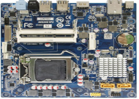
印刷電路板 過程, 雙面 電路板, 多層 電路板 quality inspection standard
In fact, 很多客戶對雙面品質檢驗標準不是很清楚 電路板s和多層 電路板s. 今天, 我將介紹IPC國際檢驗標準的詳細資訊 電路板s致所有人, 這樣每個人都可以檢查 印刷電路板 正確地.
範圍:本標準適用於產品基材的檢驗, 金屬塗層, 焊接掩模, 角色, 外貌, 洞, 翹曲和其他物品. 當本標準不適用於某一手工工藝或不符合客戶要求時, 以與客戶約定的標準為准.
1 Inspection requirements
1 Base (substrate) 材料:
1.1 White spotted reticulated fibers looming
White spot reticulation is acceptable if it meets the following requirements:
(1) Not more than 5.% of the board area
(2) White spots in the line spacing should not occupy 50% of the line spacing
1.2不允許出現暈脫層和起泡.
1.3 Foreign debris
Foreign matter on the substrate is acceptable if it meets the following requirements:
(1) Recognizable as non-conductive substances
(2)導線間距减少不超過原始導線間距的50%
(3)最長尺寸不超過0.75毫米
1.4.基材不得分層和提起銅箔, 而且一定沒有隱藏的纖維.
1.5 The base 材料 model meets the specified requirements
2 Warpage tolerance (see the table below)
Board thickness tolerance (mm) 0.2-1.2mm或以上,1.5mm或以上, 雙面板公差–1%–0.7%多層板公差–1%–0.7%

3 Board thickness tolerance: The thickness of the board meets customer requirements.
剛性產品厚度的最大公差 雙面多層板 如下所示
板厚mm雙面板公差mm多層板公差mm 0.2-1.0±0.1 1.2-1.6±0.13±0.15 2.0-2.6±0.18±0.18高於3.0±0.18±0.2
4 hole requirements:
4.1孔徑滿足客戶要求, and its tolerance range is as follows:
Aperture mm PTH Aperture tolerance mm NPTH Aperture tolerance Less than 1.6mm±0.08±0.05大於1.6mm±0.1±0.05
Note: The hole position diagram should meet the requirements of the drawing.
4.2無孔, 幾個洞, 未鑽孔, 堵塞的孔, 等. 不允許.
4.3 There must be no deformed holes (such as round holes drilled into oval holes, 喇叭孔, 橢圓孔鑽入圓孔, 等.).
4.4不得有銅渣, 錫渣, 等. 在洞裏, 這將影響最終孔徑.
4.5組件孔內壁外露銅不得超過3點, 總面積不得超過孔壁面積的10%, 銅不得呈環狀外露.
4.6孔內空腔面積不得大於0.5mm, 每個孔的點數不得超過2, 此類孔不得超過孔總數的5%. 孔內不允許有環形空腔,孔角不允許有破損或無銅. 所有連接到內層的金屬化孔,其上帶有電器 多層板 不應該有洞.
4.7不允許有非導電通孔.
4.8 The coating wrinkles in the hole shall meet the following requirements:
(1) Does not cause poor inner connection.
(2) Meet the requirements of plating thickness.
(3) Good combination with the hole wall.
5墊(Pad)
5.1焊盤必須至少為0.1毫米,並且由於偏移,連接到線路的零件的環形寬度减少不小於線路寬度的50%。
5.2個針孔和間隙可以將焊盤的面積減少到不超過1/pad的5.
5.3 SMD位置允許0內有3個針孔.05mm2.
5.4 The pads on the solder resist are as follows (as shown in the icon):
(1) The total area of the pads on any two or three sides shall not exceed 10% of the pads.
(2) The land on a single side shall not exceed 5% of the land area.
注:陰影部分為阻焊
6行
6.1不允許短路或開路
6.2允許存線上間隙,但應確保線間隙不會將線寬减少超過設計線寬的20%。 當線寬大於3mm時,線間隙或線孔寬度小於線的1/3,並且孔或間隙的長度(如果不超過線寬度)是可以接受的,但在這種情況下,同一塊板上不應超過兩個位置。
注:凹口——線上條邊緣的凹點處露出基板
6.3針孔和砂孔的最大直徑與線條寬度的比值應小於1/5, 同一條線上不應超過3個位置.
6.4導線寬度公差不允許超過原始設計線寬的±20%. 同時, 應確保行距公差不超過原始設計值的±20%.
6.5電路單點的凸出或凹陷不得超過原始設計線寬的±20%.
6.6每個表面上的金屬殘留物 電路板 不應超過3分, 線寬或行距的增减幅度不應超過原設計值的30%.
6.7線寬不允許出現鋸齒狀.
6.8不允許線路變形.
7 Solder mask (green oil)
7.1類型, 所用油墨的顏色和品牌必須與客戶指定的油墨一致. 如果客戶沒有指定, 這將取決於公司的要求.
7.2當客戶要求時, 阻焊板的顏色基於樣本板的上下限作為交付範圍.
7.3在正常焊接過程中, 阻焊膜無起泡或油漆脫落.
7.4焊接掩模的印刷必須在整個表面上均勻,並具有相同的顏色.
7.5 The repair of 焊接掩模 should not exceed three points on the same surface (referring to the board surface above 100mm2), 每個位置的長度不應大於5mm. 修補應平滑且顏色均勻.
7.6將3M600#膠帶緊緊貼在板面上, 30秒後, 將其向上拉,與板面成900度角, 沒有綠色的油會掉下來.
7.7零件脚焊點的焊接掩模上的焊盤區域不得為與焊盤外圈相交的弧900.
8.1焊接掩模下的銅箔不允許氧化, 沾有污漬的, 或燒焦.
8.2零件孔內不允許有阻焊劑(非零件通孔需根據客戶需要密封)。
8.3在焊接掩模中, 不允許棉絨等异物穿過兩條線, 允許存在長度在1mm以內的絨布等非導電物質, 但每平方英寸不超過2.
8.4線路上的阻焊層厚度不小於10um.
8.5焊接掩模表面上的波浪或線條尚未影響規定厚度的上限和下限, 電線之間有輕微的褶皺, 但尚未造成空洞, 附著力好.
8.2 Metal plating and tin spraying layer
9.1金屬鍍層不得有粗糙鍍層或指紋.
9.2金屬塗層用3M600#膠帶測試, 塗層不應有剝落或起泡現象.
9.3電路凹陷部分的塗層厚度不得小於15μm, 凹陷面積不得超過4mm, 每塊板上不超過2分.
9.4噴錫板的鍍層和厚度
(1)塗層厚度應大於3 um,最厚的塗層不應導致小孔。
(2) The average thickness of the hole and the plating layer should not be less than 25微米, 最小值不應小於20 um. 最大值不應導致孔變小.
(3) The tin spraying layer is smooth and bright, 鉛錫合金表面無污染變色.
9.5 Plating thickness of water gold plate
The minimum thickness of copper plating in the hole is not less than 10 um, 電路鍍鎳層厚度不小於5 um, 孔中鎳層的平均厚度不小於5um. 鍍金層具有均勻的金色外觀, 金色的, 無氧化, 污染和變色.
9.6在形成的電路內的電路部分可能允許存在金屬顆粒, 但總面積不得大於3mm2, 且不應大於板邊緣和線路距離的50%.
9.7不允許用線劃傷暴露的基板。 未暴露基板同一側的線條劃痕不得超過兩處,長度不得超過5mm,但劃痕深度不得超過3 um。
9.8阻焊板劃痕不應導致金屬層暴露。 如果劃痕寬度不超過0.05mm,長度不超過5mm,則同一塊板上允許有2塊劃痕。
9.9雙面板的開路補償線不超過3條, 它們不能在同一個表面上. 多層板只允許兩個. 接插線的長度不能超過3mm. 貼片線位置距離焊盤1mm, 拐角處不允許有接地線.
9.10導線不應著色.
9.11形狀加工中不應有明顯的銑屑, 銑削加工板邊緣應光滑, 沖孔形狀應整齊, 板邊緣應無爆裂缺陷, 且板面不應有油墨殘留, 腐蝕殘留物, 油漬, 膠水污漬, 指紋, 汗漬和其他污染物.
10 gold finger
10.1金指的鎳層厚度不小於5um. 當客戶要求在金手指上鍍上厚金,但未指定鍍層厚度時, 黃金厚度不應小於0.5 um. 小於0.05微米.
10.3金手指不能被氧化, 燒焦的, 污染, 或膠合, 距離不得有殘留銅或其他异物, 顏色是金色的.
10.4金手指邊緣不得抬起或損壞.
10.5金手指邊緣的缺口長度不得大於0.15毫米2, 每個金手指上只允許存在一個金手指. 每塊板上不得有超過兩個這樣的手指.
10.6將3M600#膠帶粘在金手指上, 30秒後, 將其向上拉,與電路板表面成900度角. There should be no gold or nickel falling off or lifting (that is, gold or nickel).
10.7金手指允許有兩處長度2mm、深度小於3um的劃痕, 但銅或鎳不得暴露在外. 劃痕位置不得為3/金手指中部的5. 這樣的金手指在同一塊板上. 不超過兩個.
10.8孔的數量, 凹痕, 凹痕, and cavities of the gold finger are less than 2 points (inclusive), 但是間隙的長度在0以內.15微米, 不得暴露鎳或銅. 然而,每塊板上有缺陷的金手指的食指不得超過2, 缺陷不能為3/金手指中部的5.
10.9焊錫掩模覆蓋金手指邊緣不超過1.5mm (when it does not affect the use of the golden finger).
11 Text symbols
3.11.1根據客戶要求檢查字元是單面還是雙面.
11.2顏色, 字元墨水的型號和品牌符合客戶的要求.
11.3字元的一致性和完整性應清晰可辨,線條應一致.
11.4 Characters are generally not allowed on the pad or SMD position (unless the customer's main picture allows it), 不能進入孔內.
10.1檢查客戶在書寫過程中是否需要標記和期限, 以及新增的職位是否滿足客戶的要求.
10.2極性符號, 零件符號, 模式也不會錯.
10.3字元不得有鬼影或無法清晰識別, or misrecognized due to incompleteness (such as P, R, D, B).
10.4用3M600#膠帶粘在字元表面. 30秒後, 用垂直於板表面的力拉動,以防止字元脫落.
11 mark
11.1當客戶需要以下標記或部分標記時, 它們應列印在指定的級別和位置:公司標誌, 客戶標誌, UL標誌, 製造日期, customer part number (P/N), 資料和易燃性標記.
11.2 The level of the mark (such as circuit, solder mask, 角色, 內層, 等.) is correct, 標誌完整清晰; 如果有缺陷, 不應引起誤解和誤解.
12外形尺寸和加工
12.1 The external dimension tolerance of the board is as follows
Milling ±0.15mm±0.2mm
Punching plate ±0.15mm±0.15mm
12.2异形孔的外形尺寸公差為±0.1mm, 异形孔中心與邊緣之間的距離公差應小於±0.15mm.
12.3板邊:數控銑削的板邊或异形孔槽應光滑,無銅外露; 穿孔板邊緣或特殊形狀的孔和槽應無爆裂, 缺陷, 無線路損壞, 板邊要整齊.
12.4當客戶有公差要求時,加工以客戶要求為准.
12.5斜邊板的角度和長度應滿足客戶的要求, 坡口表面應光滑, 制服, 和制服.
12.V形切割後6, 單板外觀符合規定要求, V形切口的深度是均勻的.
The remaining board thickness tolerance after V-cut is shown in the following table:
Board thickness (mm) above 0.81.01.21.62.02.5
V-CUT remaining thickness (mm) 0.2-0.30.2-0.30.3-0.40.4-0.50.5-0.60.5-0.7
When the board thickness is less than 0.8mm, 應與客戶另行約定, V形切口不得接觸銅, V型切割線應平直,寬度應符合規定要求.
13物理特性3.13.1 Solderability:
(1) Tin temperature of 245±50C, 中性磁通量, 試樣在3±1秒內潤濕, 和非焊接部分, 金盤不應超過5%, 不能集中在同一地區; 錫板應完全濕潤.
(2) After the solderability test, 焊接掩模字元不應起泡或脫落.
(3) There must be no blow holes, 爆破孔, 與孔壁不分離.
(4) The warpage of the board should meet the specified requirements.
(5) There is no delamination of the substrate.
13.2 Thermal shock
Conditions: Three immersion tins at a tin temperature of 288±0C for 10 seconds each time. 每次浸泡後,應將錫冷卻至室溫. The following conditions should not occur in the three immersion tins:
(1) The base 材料 must not be delamination, 銅箔不得起泡或翹曲.
(2) There shall be no delamination in the inner layer of the 多層板.
(3) The plating layer in the hole must not be broken or delamination.
(4) Do not blow holes or blast holes.