電磁相容性EMC是指 印刷電路板設備 或系統在其電磁環境中按照要求運行,並且不會對其環境中的任何設備產生不可容忍的電磁干擾. 一方面, 有必要盡可能减少電磁頻譜的發射, 另一方面, 有必要保護設備免受電磁干擾. 電磁干擾源, 耦合路徑和接收器是形成干擾的3個要素, 缺少其中任何一個都不會造成干擾.

電磁相容性設計與特定電路密切相關. 為了進行電磁相容設計, 這個 印刷電路板設計工程師 needs to minimize the radi公司ation (radio frequency energy leaking from the product) and enhance its radiation (the energy entering the product) The susceptibility and anti-interference ability. 對於低頻的公共傳導耦合和高頻的公共輻射耦合, 必須充分注意切斷耦合路徑 印刷電路板設計. 有3個基本原則 印刷電路板抗干擾設計: 印刷電路板 抑制干擾源, 切斷干擾傳播路徑, 提高了敏感器件的抗干擾效能.
1. 印刷電路板設計 suppresses interference sources
Suppressing the interference source is to reduce the du/dt (digital device voltage change rate), di/dt (digital device current change rate) of the interference source as much as possible. 這是抗干擾設計中最優先、最重要的原則, 它通常具有事半功倍的效果. 减少du/干擾源的dt主要通過在干擾源兩端並聯連接電容器來實現. 减少di/通過將電感或電阻與干擾源回路串聯並添加續流二極體來實現干擾源的dt.
2. Cut off the interference propagation path
(1) Fully consider the impact of the power supply on the microcontroller. 如果供電良好, 整個電路的抗干擾問題將解决一半以上. 許多單片機對電源雜訊非常敏感, 電源應新增濾波電路或電壓調節器,以减少電源雜訊對單片機的干擾.
(2) Pay attention to the crystal oscillator wiring. 晶體振盪器盡可能靠近微控制器的引脚, 時鐘區域用地線隔離, 晶體振盪器外殼接地並固定.
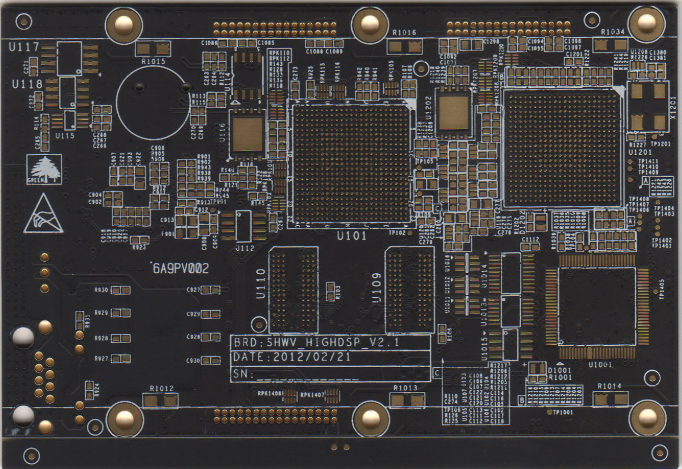
(3) Reasonable division of the circuit board, 如强弱訊號, 數位和類比信號. Keep interference sources (such as motors, relays) away from sensitive components (such as single-chip microcomputers) as far as possible.
(4) Separate the digital area from the analog area with a ground wire, 將數位接地與類比接地分開, 最後在一點將其連接到電源接地. A./D, D/晶片佈線也基於此原理.
3. 提高中敏感設備的抗干擾效能 印刷電路板設計
提高敏感設備的抗干擾效能是指儘量減少從敏感設備一側拾取的干擾雜訊,並儘快從异常情况中恢復的方法. Common measures to improve the anti-interference performance of sensitive devices:
(1) For the idle I/O單片機埠, 不要浮動, 但應接地或連接到電源. 其他集成電路的空閒端子接地或連接到電源,而不改變系統邏輯.
(2) The use of a power supply monitoring circuit for the single-chip microcomputer can greatly improve the anti-interference performance of the entire circuit.
(3) On the premise that the speed can meet the requirements, 儘量降低單片機晶體振盪器頻率,選擇低速數位電路.
(4) IC devices should be soldered directly on the circuit board as much as possible, IC插座應儘量少用.
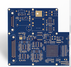
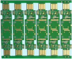
印刷電路板打樣 refers to the trial production of 印刷電路板 批量生產前. 主要應用是電子工程師在設計電路並完成測試後的小批量試生產過程 印刷電路板。 此過程屬於 印刷電路板打樣 as we understand it before the product design is confirmed and tested.
印刷電路板打樣表面 treatment generally uses hot air leveling and spraying tin, 全板鍍鎳和鍍金, organic solderability preservative (OSP), 和浸沒銀
, 浸沒金, 浸入式錫, 電鍍硬金, 化學鎳鈀金和其他工藝,以確保良好的可焊性或電力效能, 這些過程需要充分考慮服務提供者的生產實力和服務水平.