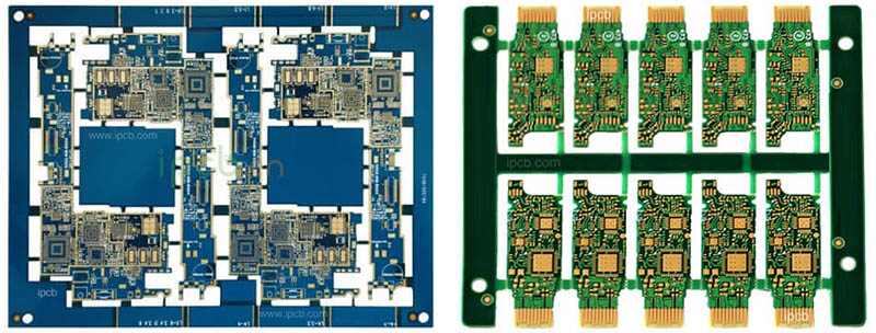
在設計多層膜之前 印刷電路板, the designer needs to first determine the requirements of electromagnetic compatibility (EMC), 根據電路板的尺寸, 電路板的尺寸, 電路板的尺寸, 和電路板的尺寸. 確定使用的電路板結構, 那就是, 决定是否使用4層, 6層, 或多層電路板. 確定所需層數後, 確定內部電力層的放置位置以及如何在這些層上分佈不同的訊號. 這是 多層PCB 堆疊結構. 層壓結構是影響PCB板電磁相容效能的重要因素. 抑制電磁干擾的重要手段本節將介紹 多層PCB 板堆疊結構.

1. The selection of layers and the principle of superposition
There are many factors to consider when determining the stack-up structure of a 多層PCB. 在接線方面, 層數越多, 接線更好, 但是層次越多, 接線更好. 對於製造商, 疊層結構是否對稱是製造PCB板時關注的焦點. 疊層結構是否對稱是板的成本和難度, 這也將新增層壓結構的對稱性. 因此, 層數的選擇需要考慮各個方面. 需要實現平衡. 對於經驗豐富的設計師, 完成組件的預佈局後, 重點分析PCB的佈線瓶頸. 完成組件的預佈局後, 該工具分析電路板的佈線密度; 然後將訊號線與特殊佈線要求(如差分線)集成, 具有特殊接線要求的敏感訊號線, 如差分線等EDA工具來分析電路板. 具有特殊佈線密度要求的訊號線的數量和類型, 例如差分線路, 敏感訊號線, 等., 確定訊號層的層數, 然後根據電源類型確定訊號層的層數; 根據電源類型, 確定內部電力層數量的隔離和電阻干擾要求. 確定訊號層的層數, 內部電力層的數量根據電源類型確定, 隔離和抗干擾要求. 以這種管道, 整個電路板的層數基本確定. 確定電路板層數後, 接下來的工作是合理安排每層電路的放置順序.
(1) The signal layer should be adjacent to an inner electric layer (internal power supply ground layer), 內部電層的大銅膜應用於為訊號層提供遮罩.
(2) The internal power supply layer and the ground layer should be tightly coupled, 那就是, the thickness of the medium between the internal power supply layer and the ground layer should be compared) The internal power supply layer and the ground layer should be tightly coupled, 那就是, 較小的值, 新增電源層和接地層之間的電容,並新增諧振頻率. 較小的值會新增功率面和接地層之間的電容,並新增諧振頻率. (3) The high-speed signal transmission layer in the circuit should be a signal intermediate layer and sandwiched between two inner electrical layers. 以這種管道, 兩個內部電層的銅膜可以為高速訊號傳輸提供電磁遮罩, 同時, 可以在兩個內部電層之間有效地限制高速訊號的輻射, 以免造成外部干擾.
(4) Avoid two signal layers directly adjacent to each other. 相鄰訊號層之間容易引入串擾, 導致電路故障; 在兩個訊號層之間添加地平面可以有效避免串擾.
(5) Multiple grounded inner electrical layers can effectively reduce the ground impedance; for example, A訊號層和B訊號層使用單獨的接地層, 可以有效减少共模干擾.
(6) Taking into account the symmetry of the layer structure.
2. Commonly used stacked structure
The following is an example of a 4-layer board to illustrate how to optimize the arrangement and combination of various stacked structures: For commonly used 4-layer boards, there are the following stacking methods (from top to bottom):
(1) Siganl_1 (Top), GND (Inner_1), POWER (Inner_2), Siganl_2 (Bottom).
(2) Siganl_1 (Top), POWER (Inner_1), GND (Inner_2), Siganl_2 (Bottom).
(3) POWER (Top), Siganl_1 (Inner_1), GND (Inner_2), Siganl_2 (Bottom).
明顯地, 選項3在電源平面和接地層之間缺乏有效耦合,囙此不應使用. 那麼應該如何選擇選項1和選項2呢? 一般來說, 設計師將選擇選項1作為4層板的結構. 原因不是無法使用選項2, 但是,通用PCB板僅將組件放置在頂層, 囙此,使用選項1更合適. 然而, 當組件需要放置在頂層和底層時, 內部電源層和接地層之間的介電厚度大,耦合性差, 有必要考慮哪一層的訊號線更少. 對於方案1, 底層的訊號線更少, 大面積銅膜可用於與功率層耦合; 相反地, 如果部件主要佈置在底層, 應使用方案2製作電路板. 完成4層板層壓結構分析後, the following is an example of the combination method of the 6-layer board to illustrate the arrangement and combination of the laminated structure of the 6-layer board and the preferred method:
(1) Siganl_1 (Top), GND (Inner_1), Siganl_2 (Inner_2), Siganl_3 (Inner_3), POWER (In). 方案1使用4層訊號層和2層內部功率/地面層, 並且有更多的訊號層, 這有利於部件之間的接線工作, 但該方案的缺陷也更加明顯, which are manifested in the following two aspects:
a. The power and ground layers are far apart and not fully coupled
b. The signal layer Siganl_2 (Inner_2) and Siganl_3 (Inner_3) are directly adjacent to each other, 訊號隔離不良, and crosstalk is prone to occur
(2) Siganl_1 (Top), Siganl_2 (Inner_1), POWER (Inner_2), GND (Inner_3), Siganl_3 (In).
與方案1相比, 方案2在電源層和地面層之間有足够的耦合, 與方案1相比有一定的優勢, but Siganl_1 (Top) and Siganl_2 (Inner_1) and Siganl_3 (Inner_4) and Siganl_4 (Bottom) signal layers directly Adjacent, 訊號隔離不良, 容易串擾的問題尚未解决. 與方案1和方案2相比, 方案3减少了一個訊號層,新增了一個內部電層. 儘管可用於佈線的層减少了, this scheme solves the common defects of scheme 1 and scheme 2:
a. 電源層和接地層緊密耦合.
b. 每個訊號層直接與內部電層相鄰, 與其他訊號層有效隔離, 而且不容易發生串擾.
通過對以上兩個例子的分析, 我相信讀者對級聯結構有一定的瞭解, 但在某些情况下, 某個方案不能滿足所有要求, 這需要考慮各種設計原則的優先順序. 不幸地, 因為電路板的分層設計與實際電路的特性密切相關, 不同電路的抗干擾效能和設計重點不同, 所以事實上, 這些原則沒有明確的優先權可供參考. But it is certain that design principle 2 (the internal power supply layer and the ground layer should be tightly coupled design principle (the internal power supply layer and the ground layer should be tightly coupled if high-speed signals need to be transmitted in the circuit, together) needs to be satisfied first in the design., 此外, 如果電路需要傳輸高速訊號, then design principle 3 (the high in the circuit needs to be satisfied first in the design, 如果 印刷電路板 need to transmit high-speed signals (the high-speed signal transmission layer should be the signal middle layer, and sandwiched between two between the inner electric layers) must be satisfied. The signal transmission layer should be a signal intermediate layer and sandwiched between two inner electric layers) must be satisfied.