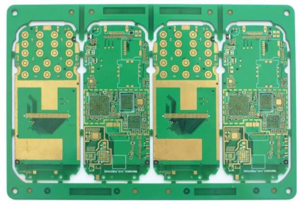
干渉防止設計 高周波回路基板
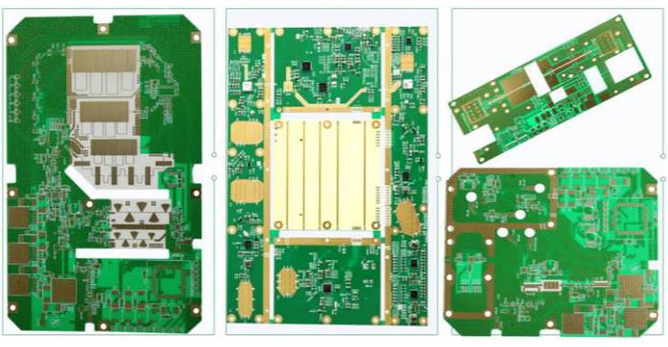
通信技術の発展, 無線高周波回路技術はますます広く使われている. 高周波回路の性能指標は製品全体の品質に直接影響する. コンポーネントのレイアウトおよび配線は、アンチジャミング設計の目的を達成するために回路の性能指標を最大化することができる.
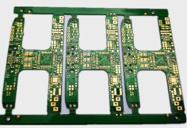
1. Layout of components
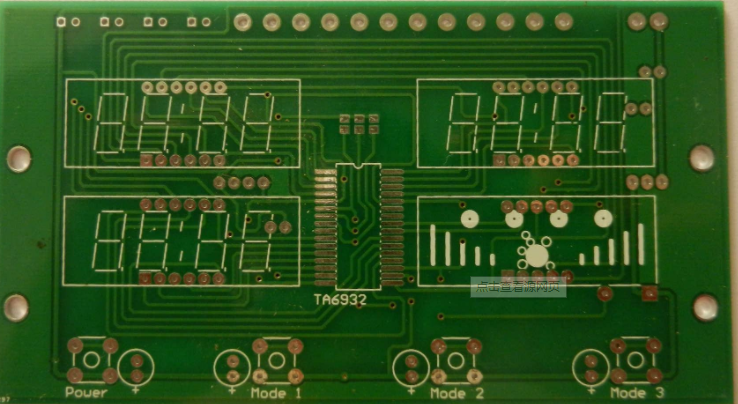
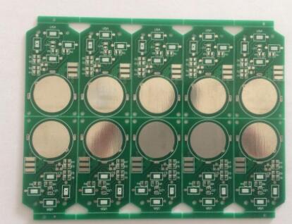
Since the surface mount chip generally uses infrared furnace heat flow welding to realize the welding of components, the layout of the components affects the quality of the solder joints, which in turn affects the yield of the product.
設計時 高周波回路s, in addition to considering the layout of ordinary PCB設計, how to reduce the mutual interference between various parts in the high-frequency circuit, 回路自体の他の回路への干渉を減らす方法, and the circuit itself Anti-interference ability.
高周波回路の効果は、高周波回路基板自体の性能指数に依存する, しかし、主にCPU処理ボードとの相互影響に依存する, それで、PCBを設計するとき、レイアウトは妥当です. レイアウトの一般的な原則は、コンポーネントができるだけ同じ方向に配置する必要があります, and the poor soldering phenomenon can be reduced or even avoided by selecting the direction of the PCB entering the soldering system;
Details in the layout:
1) First determine the position of the interface components with other PCBボードs or systems on the PCBボード, and you must pay attention to the coordination problems between the interface components (the direction of adding components, etc.);

2) Because the volume of the handheld products is very small, 部品の配置は非常にコンパクトである, だから大きなコンポーネント, 優先順位は対応する位置に与えなければならない, and the mutual cooperation should be considered;
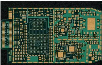
3) Carefully analyze the circuit structure, divide the circuit into blocks (add high-frequency amplifier circuits, 混合回路, and demodulation circuits, etc.), separate strong and weak electrical signals as much as possible, アナログ信号回路からデジタル信号回路を分離する, 同じ機能を完成する回路は、信号ループ領域を減少させるためにできるだけ特定の範囲内に配置されるべきである回路の各部分のフィルタネットワークを近くに接続しなければならない, which can not only reduce the radiation height, but also reduce the probability of interference. Improve the anti-interference ability of the circuit;
4) Groups are grouped according to the different electromagnetic compatibility sensitivity of the unit circuits in use.
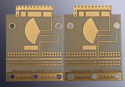
2. Wiring
After the layout of the components is basically completed, 配線を開始できる. The basic principle of wiring is: When the assembly density permits, 低密度配線設計を選ぶ, そして信号配線はできるだけ厚い, これはインピーダンス整合に役立っている.
デザインの場合 高周波回路, comprehensively consider the direction, width, 信号線の線間隔, and make reasonable wiring. 配線, すべての跡を離れて PCBボード 約2 mm, ワイヤ破損や隠れた危険性を避けるために PCBボード 作られる.
電力線は、ループ抵抗を低減するためにできるだけ広くなければならず、同時に、電力線と接地線の方向を、データ干渉の方向と一致させ、干渉防止能力を向上させる信号線はできるだけ短くする必要があります、そして、ビアの数は最小にされなければなりません;構成要素間の配線が短く、分布パラメータ及び相互電磁干渉を低減する互換性のない信号線は互いに可能な限り遠く離れていなければならなくて、平行配線を避けるようにしようとします、そして、両側の信号線は互いに垂直でなければなりません;配線時には、角が必要な場合は135°°の角度を使用し、直角に曲がることを避ける。