PCBボードが完全に電気的に安定していることを望んでいますが、実際の状況はそうではありません。現実世界は完全な導体と絶縁体で構成されているわけではありません。それらは真空に囲まれており、電界は現実システムの導体と基板と相互作用します。ICを設計するにしてもPCBにしても、不完全な電子製品の重要な影響:エレクトロマイグレーションを考慮しなければならない。エレクトロマイグレーションとは?なぜエレクトロマイグレーションが発生したのか?さらに重要なのは、どのように予防するか?簡単なPCBとICのエレクトロマイグレーション分析。目的は、これらのデバイスが異なる条件で短絡したり、オープンしたりするのを防ぐことです。このためにいくつかの業界標準が制定されている。これらの基準と、移行がどのようにして新しいデバイスの障害を引き起こすのかを理解する必要があります。
Electromigration in electrons
As more components are stacked in a smaller space, the electric field between two conductors with a specified potential difference becomes larger. This leads to some safety problems in high-voltage electronic equipment, especially electrostatic discharge (ESD). The high electric field between two conductors separated by air will cause the air to undergo dielectric breakdown, thereby generating an arc and a current pulse in the surrounding circuit. To prevent these discharges in PCB boards or other equipment, conductors need to be separated by a certain spacing, which depends on the potential difference between the conductors. The above gap distance is important for safety and preventing equipment failure, but the distance across the substrate is also important. Another point to consider is the distance between conductors across the dielectric. In PCB, this is called creepage distance. When the distance between conductors is small, the electric field may be large, resulting in electromigration. When the current density in a conductor is large (in IC), or when the electric field between two conductors is large (in PCB), the mechanism of driving electromigration can be described as exponential growth. To prevent electromigration, you can use three levers to pull in your design:
導体間の間隔を増やす(PCBボード内)、導体間の電圧を下げる(PCBボード内)、デバイスを低い電流(IC内)で動作させます。
Electromigration in IC: open circuit and short circuit
IC相互接続では、主な力は2つの導体間の電界とそれに続くイオン化ではない。逆に、固体エレクトロマイグレーションは高電流密度での電子運動量移動(散乱)に起因し、これにより金属は導電経路(この場合、金属相互接続自体)に沿って移動する。移動速度は相互接続温度の上昇とともに増加した。銅の電気移動にかかる力は以下の通りである。風力とは、格子中の金属原子からの電子の散乱によって金属イオンに加わる力を指す。この繰り返しのイオン化と運動量は自由金属イオン上に移動し、アノードへの拡散をもたらす。この移動過程は活性化エネルギーを有し、金属原子に移動するエネルギーがアレニウス活性化過程を超えると、方位拡散が始まり、濃度勾配(フェナントリック法則)の案内の下で行われる。金属が導体表面に引っ張られると、2つの導体をブリッジできる構造を構築し始め、短絡を引き起こす。また、相互接続アノード側の金属を使い果たし、開放をもたらします。以下のSEM画像は2つの導体間の拡張電気移動の結果を示している。金属が表面に沿って移動すると、ギャップ(開回路)が残ったり、隣接する導体に接続されたホイスカ(短絡)が発生したりします。オーバーホールを有する極端な場合、電気移動は被覆層下の導体を枯渇させる可能性さえある。
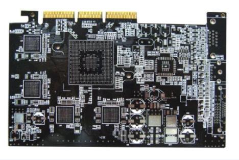
Electromigration in PCB: dendritic growth
Similar effects occur in PCB boards, resulting in two possible forms of electromigration:
As described above, electromigration along the surface, the formation of semiconductor salts, leads to the electrochemical growth of dendritic structures. These effects are controlled by different physical processes. The current density between the two conductors may be low because the size of the metal traces is very large compared to the cross section of the IC interconnect. In this case, migration will occur at high current density, resulting in the growth of the same type of stubs over time. On the surface layer, oxidation may subsequently occur as the conductor is exposed to air. In the second case, electromigration is an electrolytic process. This field drives electrochemical reactions in the presence of water and salt. Electrolytic electromigration requires water on the surface and high direct current between the two conductors, which will drive the electrochemical reaction and the growth of dendritic structures. The migrated metal ions are dissolved in the aqueous solution and diffused over the entire insulating substrate. Increasing the distance between adjacent conductors reduces the electric field between them, thereby suppressing the reaction of driving electrolytic electromigration. Electromigration analysis in the new layout needs to check the design to ensure that the trace gap does not violate design rules or industry standards. If you can use some basic PCB board or IC layout tools, you can check the layout against these rules and find any violations. With the shrinking of IC and
PCB board, electromigration analysis will only become more and more important to ensure reliability.