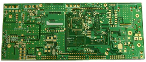
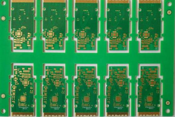
Standard for surface coa(錫)g (plating) coating of PCB電路板
從PCB電路板焊盤焊接元件的工藝和檢驗來看,PCB電路板焊盤表面塗層(電鍍)標準主要有以下五個方面。
-耐熱性
在高焊接溫度下, the surface coating (plating) coating can still protect the copper surface of the PCB circuit board pad from air oxidation and allow the soldering 材料 to enter the copper (or metal) surface to establish a connection. The heat resistance of organic surface coating (plating) refers to the performance of its melting point and thermal decomposition (volatility) temperature. 其熔點應接近或略低於 PCB焊接材料 (tin), but its thermal decomposition The temperature ( 350°C) should be much higher than the melting point temperature and welding temperature of the welding 材料 to ensure that the copper surface does not generate air oxidation during welding. 金屬表面塗層的耐熱性沒有這個問題.
-覆蓋範圍
對於有機耐熱可焊性塗層(包括助焊劑),它可以在焊接之前和焊接過程中完全覆蓋在銅焊盤的表面,而不會被空氣氧化和污染,只有當熔化的焊料焊接到銅焊盤的表面時,它才能遊走、分解和揮發,並漂浮(覆蓋)在焊點的表面上。

因此, 為了確保熔化的焊接材料完全焊接在耦合盤上, 熔融有機表面塗層的表面張力必須低,分解溫度必須高,以確保焊接前和焊接過程中良好的覆蓋. 同時, its specific gravity is much smaller than that of the molten solder 材料 (tin) to ensure that the molten solder 材料 squeezes and penetrates the copper surface. 因此, 有機表面塗層的覆蓋範圍是指其在焊接溫度下的溫度. 表面張力, 比重和其他特性. 在焊接過程中,金屬表面塗層部分熔化到焊接材料中或在阻擋層表面上,以建立連接.
遺骸
有機耐熱可焊性塗層(鍍層)的殘留物是指焊接材料焊接後在焊盤或焊點上的殘留物。 在正常情况下,這些殘留物是有害的(如有機酸或鹵化物等),應清除,囙此應在焊接後採取清潔措施。 現時,沒有清潔的焊接技術,因為有機表面塗層(電鍍)在焊接後殘留很少(大部分已分解和揮發)。
-腐蝕性
有機耐熱可焊性塗層(電鍍)的腐蝕性是指焊接材料焊接後對PCB電路板表面的腐蝕,如對PCB電路板基板表面和金屬層的腐蝕。 這是因為有機耐熱可焊性塗層(電鍍)中或多或少含有鹵化物或有機酸(主要是為了進一步清潔銅墊上的殘留氧化物和污染物),但焊接後酸性物質的存在是危險的。 除分解和揮發外,還必須清潔和去除。
–環境保護
PCB表面塗層(電鍍)的環境保護是指:在建立塗層過程中產生的廢渣和焊接後清潔的廢液應易於處理、成本低且不污染環境。
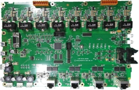
PCB巨磁電阻效應及層結構分析
所謂巨磁電阻效應是指當有外磁場時,與沒有外磁場時相比,資料的電阻率發生顯著變化的現象. It is generally defined as GMR = where (H) is the resistivity of the 材料 under the action of the magnetic field H (0) refers to the resistivity of the 材料 without the action of an external magnetic field. The huge change in the resistance of some magnetic 材料 caused by an external magnetic field (called the giant magnetoresistance effect) is an important content in magnetoelectronics. 室溫下具有巨磁電阻效應的巨磁電阻資料有很多種, 例如, 多層巨磁電阻資料, 顆粒巨磁電阻資料, 氧化物巨磁電阻資料, 隧道結磁電阻資料.
所謂磁阻效應是指導體或電晶體的電阻在磁場作用下發生變化的現象。 巨磁電阻效應是由Peter Grünberg和Albert Fert於1988年獨立發現的。, 他們共同獲得了2007年諾貝爾物理學獎。 研究發現,在鐵/鉻和鈷/銅等磁性多層膜中,鐵磁性層由納米厚度的非磁性材料分離。 在某些條件下,電阻率的降低幅度相當大,大約是普通磁性金屬和合金材料磁電阻值的10倍。 這種現象被稱為“巨磁電阻效應”
巨磁電阻效應可以用量子力學來解釋。 每個電子都可以自旋,電子的散射速率取決於磁性材料的自旋方向和磁化方向。 自旋方向與磁性材料的磁化方向相同,電子散射率低,更多的電子通過磁性層,囙此顯示出低阻抗。 相反,當自旋方向與磁性材料的磁化方向相反時,電子散射率較高,囙此通過磁性層的電子較少,此時表現出高阻抗。
基於PCB巨磁電阻效應的感測器主要有3層傳感資料:參攷層或釘紮層, Normal Layer and Free Layer (The giant magnetoresistance effect often referred to as Free refers to the resistivity of raw 材料). 當有外部磁場時, 與沒有外部磁場時相比,有顯著變化. It is usually defined as GMR = where (H) is the resistivity of the PCB資料 under the action of the magnetic field H (0) means that there is no external magnetic field. 較低原材料的電阻率. The huge change in the resistance of some magnetic 材料 caused by an additional magnetic field (called the giant magnetoresistance effect) is an important content in magnetoelectronics. 具有巨磁阻效應的巨磁體在室溫下有多種類型的電阻原材料處於這一階段, 例如, 多層膜巨磁電阻原材料, 顆粒巨磁電阻原材料, 氧化物型巨磁電阻原材料, 隧道結磁阻原材料, 等.